参数资料
| 型号: | ISL6565BCV-T |
| 厂商: | Intersil |
| 文件页数: | 19/28页 |
| 文件大小: | 0K |
| 描述: | IC REG CTRLR BUCK PWM VM 28TSSOP |
| 标准包装: | 2,500 |
| PWM 型: | 电压模式 |
| 输出数: | 1 |
| 频率 - 最大: | 1.5MHz |
| 占空比: | 66.7% |
| 电源电压: | 4.75 V ~ 5.25 V |
| 降压: | 是 |
| 升压: | 无 |
| 回扫: | 无 |
| 反相: | 无 |
| 倍增器: | 无 |
| 除法器: | 无 |
| Cuk: | 无 |
| 隔离: | 无 |
| 工作温度: | 0°C ~ 105°C |
| 封装/外壳: | 28-TSSOP(0.173",4.40mm 宽) |
| 包装: | 带卷 (TR) |
第1页第2页第3页第4页第5页第6页第7页第8页第9页第10页第11页第12页第13页第14页第15页第16页第17页第18页当前第19页第20页第21页第22页第23页第24页第25页第26页第27页第28页
�� �
�
�ISL6565A,� ISL6565B�
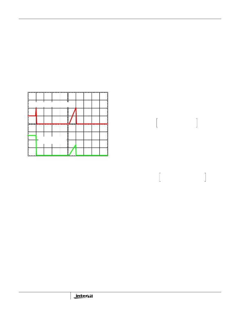
�consecutive� cycles,� the� comparator� triggers� the� converter� to�
�shutdown.�
�At� the� beginning� of� overcurrent� shutdown,� the� controller�
�places� all� PWM� signals� in� a� high-impedance� state�
�commanding� the� Intersil� MOSFET� driver� ICs� to� turn� off� both�
�upper� and� lower� MOSFETs.� The� system� remains� in� this� state�
�for� a� period� of� 4096� switching� cycles.� If� the� controller� is� still�
�enabled� at� the� end� of� this� wait� period,� it� will� attempt� a� soft-�
�start� (as� shown� in� Figure� 14).� If� the� fault� remains,� the� trip-�
�retry� cycles� will� continue� indefinitely� until� either� the� controller�
�is� disabled� or� the� fault� is� cleared.� Note� that� the� energy�
�delivered� during� trip-retry� cycling� is� much� less� than� during�
�full-load� operation,� so� there� is� no� thermal� hazard.�
�OUTPUT� CURRENT,� 50A/DIV�
�If� through-hole� MOSFETs� and� inductors� can� be� used,� higher�
�per-phase� currents� are� possible.� In� cases� where� board�
�space� is� the� limiting� constraint,� current� can� be� pushed� as�
�high� as� 40A� per� phase,� but� these� designs� require� heat� sinks�
�and� forced� air� to� cool� the� MOSFETs,� inductors� and� heat-�
�dissipating� surfaces.�
�MOSFETS�
�The� choice� of� MOSFETs� depends� on� the� current� each�
�MOSFET� will� be� required� to� conduct,� the� switching� frequency,�
�the� capability� of� the� MOSFETs� to� dissipate� heat,� and� the�
�availability� and� nature� of� heat� sinking� and� air� flow.�
�LOWER� MOSFET� POWER� CALCULATION�
�The� calculation� for� power� loss� in� the� lower� MOSFET� is�
�simple,� since� virtually� all� of� the� loss� in� the� lower� MOSFET� is�
�due� to� current� conducted� through� the� channel� resistance�
�(r� DS(ON)� ).� In� Equation� 20,� I� M� is� the� maximum� continuous�
�output� current,� I� PP� is� the� peak-to-peak� inductor� current� (see�
�Equation� 1),� and� d� is� the� duty� cycle� (V� OUT� /V� IN� ).�
�?� I� M� ?� 2� I� L� ,� PP� (� 1� –� d� )�
�P� LOW� ,� 1� =� r� DS� (� ON� )� ?� ------� ?� (� 1� –� d� )� +� --------------------------------�
�0A�
�?� N� ?� 12�
�(EQ.� 20)�
�An� additional� term� can� be� added� to� the� lower-MOSFET� loss�
�OUTPUT� VOLTAGE,�
�500mV/DIV�
�0V�
�2ms/DIV�
�FIGURE� 14.� OVERCURRENT� BEHAVIOR� IN� HICCUP� MODE�
�F� SW� =� 500kHz�
�equation� to� account� for� additional� loss� accrued� during� the�
�dead� time� when� inductor� current� is� flowing� through� the�
�lower-MOSFET� body� diode.� This� term� is� dependent� on� the�
�diode� forward� voltage� at� I� M� ,� V� D(ON)� ,� the� switching�
�frequency,� f� S� ,� and� the� length� of� dead� times,� t� d1� and� t� d2� ,� at�
�the� beginning� and� the� end� of� the� lower-MOSFET� conduction�
�interval� respectively.�
�I� PP� ?�
�I� M�
�P� LOW� ,� 2� =� V� D� (� ON� )� f� S� ?� ------� +� I� ---------� ?� t�
�?� I�
�?� d1� +� ?� ?� ------� –� ---------� ?� ?� d2�
�t�
�?� N�
�General� Design� Guide�
�PP� M�
�2� N� 2�
�(EQ.� 21)�
�This� design� guide� is� intended� to� provide� a� high-level�
�explanation� of� the� steps� necessary� to� create� a� multi-phase�
�power� converter.� It� is� assumed� that� the� reader� is� familiar� with�
�many� of� the� basic� skills� and� techniques� referenced� below.� In�
�addition� to� this� guide,� Intersil� provides� complete� reference�
�designs� that� include� schematics,� bills� of� materials,� and� example�
�board� layouts� for� all� common� microprocessor� applications.�
�Power� Stages�
�The� first� step� in� designing� a� multi-phase� converter� is� to�
�determine� the� number� of� phases.� This� determination�
�depends� heavily� on� the� cost� analysis� which� in� turn� depends�
�on� system� constraints� that� differ� from� one� design� to� the� next.�
�Principally,� the� designer� will� be� concerned� with� whether�
�components� can� be� mounted� on� both� sides� of� the� circuit�
�board,� whether� through-hole� components� are� permitted,� the�
�total� board� space� available� for� power-supply� circuitry,� and�
�the� maximum� amount� of� load� current.� Generally� speaking,�
�the� most� economical� solutions� are� those� in� which� each�
�phase� handles� between� 25A� and� 30A.� All� surface-mount�
�designs� will� tend� toward� the� lower� end� of� this� current� range.�
�19�
�The� total� maximum� power� dissipated� in� each� lower� MOSFET�
�is� approximated� by� the� summation� of� P� LOW,1� and� P� LOW,2� .�
�UPPER� MOSFET� POWER� CALCULATION�
�In� addition� to� r� DS(ON)� losses,� a� large� portion� of� the� upper-�
�MOSFET� losses� are� due� to� currents� conducted� across� the�
�input� voltage� (V� IN� )� during� switching.� Since� a� substantially�
�higher� portion� of� the� upper-MOSFET� losses� are� dependent�
�on� switching� frequency,� the� power� calculation� is� more�
�complex.� Upper� MOSFET� losses� can� be� divided� into�
�separate� components� involving� the� upper-MOSFET�
�switching� times,� the� lower-MOSFET� body-diode� reverse-�
�recovery� charge,� Q� rr� ,� and� the� upper� MOSFET� r� DS(ON)�
�conduction� loss.�
�When� the� upper� MOSFET� turns� off,� the� lower� MOSFET� does�
�not� conduct� any� portion� of� the� inductor� current� until� the�
�voltage� at� the� phase� node� falls� below� ground.� Once� the�
�lower� MOSFET� begins� conducting,� the� current� in� the� upper�
�MOSFET� falls� to� zero� as� the� current� in� the� lower� MOSFET�
�ramps� up� to� assume� the� full� inductor� current.� In� Equation� 22,�
�FN9135.4�
�December� 1,� 2005�
�相关PDF资料 |
PDF描述 |
|---|---|
| ISL6566AIRZ | IC CTRLR PWM 3PHASE BUCK 40-QFN |
| ISL6566CRZ-T | IC CTLR PWM BUCK 3PHASE 40-QFN |
| ISL6567CRZ | IC REG CTRLR BUCK PWM VM 24-QFN |
| ISL6568CRZ-T | IC CTLR PWM BUCK 2PHASE 32-QFN |
| ISL6569ACR-T | IC REG CTRLR BUCK PWM 32-QFN |
相关代理商/技术参数 |
参数描述 |
|---|---|
| ISL6565BCVZ | 功能描述:IC REG CTRLR BUCK PWM VM 28TSSOP RoHS:是 类别:集成电路 (IC) >> PMIC - 稳压器 - DC DC 切换控制器 系列:- 产品培训模块:Lead (SnPb) Finish for COTS Obsolescence Mitigation Program 标准包装:2,500 系列:- PWM 型:电流模式 输出数:1 频率 - 最大:275kHz 占空比:50% 电源电压:18 V ~ 110 V 降压:无 升压:无 回扫:无 反相:无 倍增器:无 除法器:无 Cuk:无 隔离:是 工作温度:-40°C ~ 85°C 封装/外壳:8-SOIC(0.154",3.90mm 宽) 包装:带卷 (TR) |
| ISL6565BCVZ-T | 功能描述:IC REG CTRLR BUCK PWM VM 28TSSOP RoHS:是 类别:集成电路 (IC) >> PMIC - 稳压器 - DC DC 切换控制器 系列:- 产品培训模块:Lead (SnPb) Finish for COTS Obsolescence Mitigation Program 标准包装:2,500 系列:- PWM 型:电流模式 输出数:1 频率 - 最大:275kHz 占空比:50% 电源电压:18 V ~ 110 V 降压:无 升压:无 回扫:无 反相:无 倍增器:无 除法器:无 Cuk:无 隔离:是 工作温度:-40°C ~ 85°C 封装/外壳:8-SOIC(0.154",3.90mm 宽) 包装:带卷 (TR) |
| ISL6566ACRZ | 功能描述:IC CTRLR PWM 3PHASE BUCK 40-QFN RoHS:是 类别:集成电路 (IC) >> PMIC - 稳压器 - 专用型 系列:- 标准包装:43 系列:- 应用:控制器,Intel VR11 输入电压:5 V ~ 12 V 输出数:1 输出电压:0.5 V ~ 1.6 V 工作温度:-40°C ~ 85°C 安装类型:表面贴装 封装/外壳:48-VFQFN 裸露焊盘 供应商设备封装:48-QFN(7x7) 包装:管件 |
| ISL6566ACRZ-T | 功能描述:IC CTRLR PWM 3PHASE BUCK 40-QFN RoHS:是 类别:集成电路 (IC) >> PMIC - 稳压器 - 专用型 系列:- 标准包装:43 系列:- 应用:控制器,Intel VR11 输入电压:5 V ~ 12 V 输出数:1 输出电压:0.5 V ~ 1.6 V 工作温度:-40°C ~ 85°C 安装类型:表面贴装 封装/外壳:48-VFQFN 裸露焊盘 供应商设备封装:48-QFN(7x7) 包装:管件 |
| ISL6566AIRZ | 功能描述:IC CTRLR PWM 3PHASE BUCK 40-QFN RoHS:是 类别:集成电路 (IC) >> PMIC - 稳压器 - 专用型 系列:- 标准包装:43 系列:- 应用:控制器,Intel VR11 输入电压:5 V ~ 12 V 输出数:1 输出电压:0.5 V ~ 1.6 V 工作温度:-40°C ~ 85°C 安装类型:表面贴装 封装/外壳:48-VFQFN 裸露焊盘 供应商设备封装:48-QFN(7x7) 包装:管件 |
发布紧急采购,3分钟左右您将得到回复。