参数资料
| 型号: | ISL6565BCV-T |
| 厂商: | Intersil |
| 文件页数: | 24/28页 |
| 文件大小: | 0K |
| 描述: | IC REG CTRLR BUCK PWM VM 28TSSOP |
| 标准包装: | 2,500 |
| PWM 型: | 电压模式 |
| 输出数: | 1 |
| 频率 - 最大: | 1.5MHz |
| 占空比: | 66.7% |
| 电源电压: | 4.75 V ~ 5.25 V |
| 降压: | 是 |
| 升压: | 无 |
| 回扫: | 无 |
| 反相: | 无 |
| 倍增器: | 无 |
| 除法器: | 无 |
| Cuk: | 无 |
| 隔离: | 无 |
| 工作温度: | 0°C ~ 105°C |
| 封装/外壳: | 28-TSSOP(0.173",4.40mm 宽) |
| 包装: | 带卷 (TR) |
第1页第2页第3页第4页第5页第6页第7页第8页第9页第10页第11页第12页第13页第14页第15页第16页第17页第18页第19页第20页第21页第22页第23页当前第24页第25页第26页第27页第28页
�� �
�
�ISL6565A,� ISL6565B�
�have� sufficiently� low� ESL� and� ESR� so� that� the� total� output-�
�voltage� deviation� is� less� than� the� allowable� maximum.�
�Neglecting� the� contribution� of� inductor� current� and� regulator�
�response,� the� output� voltage� initially� deviates� by� an� amount�
�Input� Supply� Voltage� Selection�
�The� VCC� input� of� the� ISL6565� can� be� connected� either�
�directly� to� a� +5V� supply� or� through� a� current� limiting� resistor� to�
�a� +12V� supply.� An� integrated� 5.8V� shunt� regulator� maintains�
�?� V� ≈� (� ESL� )� -----� +� (� ESR� )� ?� I�
�di�
�dt�
�(EQ.� 41)�
�the� voltage� on� the� VCC� pin� when� a� +12V� supply� is� used.� A�
�300� ?� resistor� is� suggested� for� limiting� the� current� into� the�
�The� filter� capacitor� must� have� sufficiently� low� ESL� and� ESR�
�so� that� ?� V� <� ?� V� MAX� .�
�Most� capacitor� solutions� rely� on� a� mixture� of� high-frequency�
�capacitors� with� relatively� low� capacitance� in� combination�
�with� bulk� capacitors� having� high� capacitance� but� limited�
�high-frequency� performance.� Minimizing� the� ESL� of� the�
�high-frequency� capacitors� allows� them� to� support� the� output�
�voltage� as� the� current� increases.� Minimizing� the� ESR� of� the�
�bulk� capacitors� allows� them� to� supply� the� increased� current�
�with� less� output� voltage� deviation.�
�The� ESR� of� the� bulk� capacitors� also� creates� the� majority� of�
�the� output-voltage� ripple.� As� the� bulk� capacitors� sink� and�
�source� the� inductor� AC� ripple� current� (see� Interleaving� and�
�Equation� 2),� a� voltage� develops� across� the� bulk-capacitor�
�ESR� equal� to� I� C,PP� (ESR).� Thus,� once� the� output� capacitors�
�are� selected,� the� maximum� allowable� ripple� voltage,�
�VCC� pin� to� a� worst-case� maximum� of� approximately� 25mA.�
�Switching� Frequency�
�There� are� a� number� of� variables� to� consider� when� choosing�
�the� switching� frequency,� as� there� are� considerable� effects� on�
�the� upper-MOSFET� loss� calculation.� These� effects� are�
�outlined� in� MOSFETs� ,� and� they� establish� the� upper� limit� for�
�the� switching� frequency.� The� lower� limit� is� established� by� the�
�requirement� for� fast� transient� response� and� small� output-�
�voltage� ripple� as� outlined� in� Output� Filter� Design� .� Choose� the�
�lowest� switching� frequency� that� allows� the� regulator� to� meet�
�the� transient-response� requirements.�
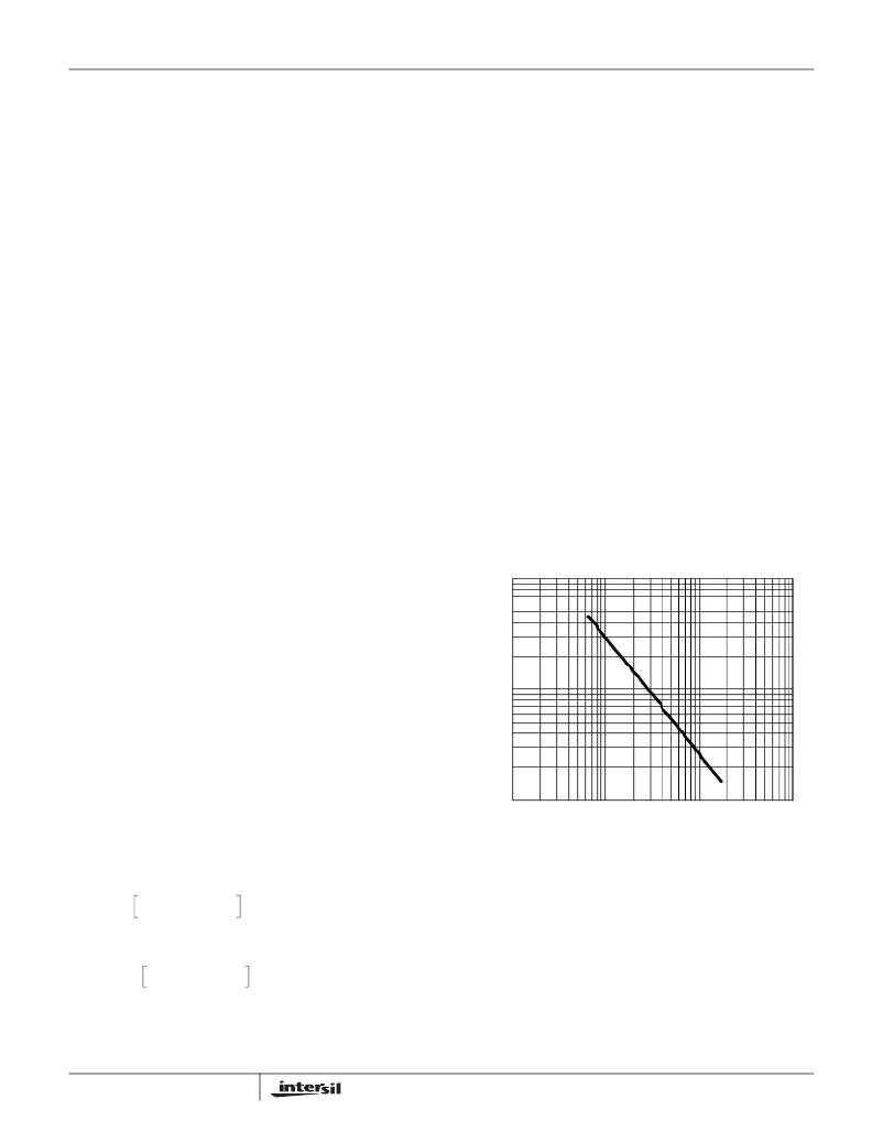
�Switching� frequency� is� determined� by� the� selection� of� the�
�frequency-setting� resistor,� R� T� (see� the� figures� labeled�
�Typical� Application� on� pages� 5� and� 6).� Figure� 18� and�
�Equation� 45� are� provided� to� assist� in� selecting� the� correct�
�value� for� R� T� .�
�–� N� V� OUT� ?� V� OUT�
�?� V�
�?� IN� ?�
�L� ≥� (� ESR� )� ------------------------------------------------------------�
�V� PP(MAX)� ,� determines� the� lower� limit� on� the� inductance.�
�(EQ.� 42)�
�f� S� V� IN� V� PP� (� MAX� )�
�R� T� =� 10�
�[� 10.7� –� 1.045� log� (� f� S� )� ]�
�(EQ.� 45)�
�1000�
�Since� the� capacitors� are� supplying� a� decreasing� portion� of�
�the� load� current� while� the� regulator� recovers� from� the�
�transient,� the� capacitor� voltage� becomes� slightly� depleted.�
�The� output� inductors� must� be� capable� of� assuming� the� entire�
�load� current� before� the� output� voltage� decreases� more� than�
�?� V� MAX� .� This� places� an� upper� limit� on� inductance.�
�Equation� 43� gives� the� upper� limit� on� L� for� the� cases� when�
�the� trailing� edge� of� the� current� transient� causes� a� greater�
�output-voltage� deviation� than� the� leading� edge.� Equation� 44�
�addresses� the� leading� edge.� Normally,� the� trailing� edge�
�dictates� the� selection� of� L� because� duty� cycles� are� usually�
�100�
�less� than� 50%.� Nevertheless,� both� inequalities� should� be�
�evaluated,� and� L� should� be� selected� based� on� the� lower� of�
�the� two� results.� In� each� equation,� L� is� the� per-channel�
�10�
�10�
�100� 1000�
�SWITCHING� FREQUENCY� (kHz)�
�10000�
�inductance,� C� is� the� total� output� capacitance,� and� N� is� the�
�number� of� active� channels.�
�FIGURE� 18.� R� T� vs� SWITCHING� FREQUENCY�
�Input� Capacitor� Selection�
�L� ≤� ---------------------� ?� V� MAX� –� ?� I� (� ESR� )�
�L� ≤� --------------------------� ?� V� MAX� –� ?� I� (� ESR� )� ?� V� IN� –� V� O� ?�
�(� ?� I� )� 2�
�2NCV� O�
�(� ?� I� )� 2�
�(� 1.25� )� NC�
�24�
�?� ?�
�(EQ.� 43)�
�(EQ.� 44)�
�The� input� capacitors� are� responsible� for� sourcing� the� AC�
�component� of� the� input� current� flowing� into� the� upper�
�MOSFETs.� Their� RMS� current� capacity� must� be� sufficient� to�
�handle� the� AC� component� of� the� current� drawn� by� the� upper�
�MOSFETs� which� is� related� to� duty� cycle� and� the� number� of�
�active� phases.�
�FN9135.4�
�December� 1,� 2005�
�相关PDF资料 |
PDF描述 |
|---|---|
| ISL6566AIRZ | IC CTRLR PWM 3PHASE BUCK 40-QFN |
| ISL6566CRZ-T | IC CTLR PWM BUCK 3PHASE 40-QFN |
| ISL6567CRZ | IC REG CTRLR BUCK PWM VM 24-QFN |
| ISL6568CRZ-T | IC CTLR PWM BUCK 2PHASE 32-QFN |
| ISL6569ACR-T | IC REG CTRLR BUCK PWM 32-QFN |
相关代理商/技术参数 |
参数描述 |
|---|---|
| ISL6565BCVZ | 功能描述:IC REG CTRLR BUCK PWM VM 28TSSOP RoHS:是 类别:集成电路 (IC) >> PMIC - 稳压器 - DC DC 切换控制器 系列:- 产品培训模块:Lead (SnPb) Finish for COTS Obsolescence Mitigation Program 标准包装:2,500 系列:- PWM 型:电流模式 输出数:1 频率 - 最大:275kHz 占空比:50% 电源电压:18 V ~ 110 V 降压:无 升压:无 回扫:无 反相:无 倍增器:无 除法器:无 Cuk:无 隔离:是 工作温度:-40°C ~ 85°C 封装/外壳:8-SOIC(0.154",3.90mm 宽) 包装:带卷 (TR) |
| ISL6565BCVZ-T | 功能描述:IC REG CTRLR BUCK PWM VM 28TSSOP RoHS:是 类别:集成电路 (IC) >> PMIC - 稳压器 - DC DC 切换控制器 系列:- 产品培训模块:Lead (SnPb) Finish for COTS Obsolescence Mitigation Program 标准包装:2,500 系列:- PWM 型:电流模式 输出数:1 频率 - 最大:275kHz 占空比:50% 电源电压:18 V ~ 110 V 降压:无 升压:无 回扫:无 反相:无 倍增器:无 除法器:无 Cuk:无 隔离:是 工作温度:-40°C ~ 85°C 封装/外壳:8-SOIC(0.154",3.90mm 宽) 包装:带卷 (TR) |
| ISL6566ACRZ | 功能描述:IC CTRLR PWM 3PHASE BUCK 40-QFN RoHS:是 类别:集成电路 (IC) >> PMIC - 稳压器 - 专用型 系列:- 标准包装:43 系列:- 应用:控制器,Intel VR11 输入电压:5 V ~ 12 V 输出数:1 输出电压:0.5 V ~ 1.6 V 工作温度:-40°C ~ 85°C 安装类型:表面贴装 封装/外壳:48-VFQFN 裸露焊盘 供应商设备封装:48-QFN(7x7) 包装:管件 |
| ISL6566ACRZ-T | 功能描述:IC CTRLR PWM 3PHASE BUCK 40-QFN RoHS:是 类别:集成电路 (IC) >> PMIC - 稳压器 - 专用型 系列:- 标准包装:43 系列:- 应用:控制器,Intel VR11 输入电压:5 V ~ 12 V 输出数:1 输出电压:0.5 V ~ 1.6 V 工作温度:-40°C ~ 85°C 安装类型:表面贴装 封装/外壳:48-VFQFN 裸露焊盘 供应商设备封装:48-QFN(7x7) 包装:管件 |
| ISL6566AIRZ | 功能描述:IC CTRLR PWM 3PHASE BUCK 40-QFN RoHS:是 类别:集成电路 (IC) >> PMIC - 稳压器 - 专用型 系列:- 标准包装:43 系列:- 应用:控制器,Intel VR11 输入电压:5 V ~ 12 V 输出数:1 输出电压:0.5 V ~ 1.6 V 工作温度:-40°C ~ 85°C 安装类型:表面贴装 封装/外壳:48-VFQFN 裸露焊盘 供应商设备封装:48-QFN(7x7) 包装:管件 |
发布紧急采购,3分钟左右您将得到回复。