- 您现在的位置:买卖IC网 > PDF目录9099 > ISPPAC-CLK5312S-01TN48C (Lattice Semiconductor Corporation)IC CLOCK PROGRAM BUFFER 48TQFP PDF资料下载
参数资料
| 型号: | ISPPAC-CLK5312S-01TN48C |
| 厂商: | Lattice Semiconductor Corporation |
| 文件页数: | 10/56页 |
| 文件大小: | 0K |
| 描述: | IC CLOCK PROGRAM BUFFER 48TQFP |
| 标准包装: | 250 |
| 系列: | ispClock™ |
| 类型: | 时钟发生器,扇出配送,零延迟缓冲器 |
| PLL: | 带旁路 |
| 输入: | HSTL,LVCMOS,LVDS,LVPECL,LVTTL,SSTL |
| 输出: | eHSTL,HSTL,LVCMOS,LVTTL,SSTL |
| 电路数: | 1 |
| 比率 - 输入:输出: | 2:12 |
| 差分 - 输入:输出: | 是/无 |
| 频率 - 最大: | 267MHz |
| 除法器/乘法器: | 是/无 |
| 电源电压: | 3 V ~ 3.6 V |
| 工作温度: | 0°C ~ 70°C |
| 安装类型: | 表面贴装 |
| 封装/外壳: | 48-LQFP |
| 供应商设备封装: | 48-TQFP(7x7) |
| 包装: | 托盘 |
第1页第2页第3页第4页第5页第6页第7页第8页第9页当前第10页第11页第12页第13页第14页第15页第16页第17页第18页第19页第20页第21页第22页第23页第24页第25页第26页第27页第28页第29页第30页第31页第32页第33页第34页第35页第36页第37页第38页第39页第40页第41页第42页第43页第44页第45页第46页第47页第48页第49页第50页第51页第52页第53页第54页第55页第56页
Lattice Semiconductor
ispClock5300S Family Data Sheet
18
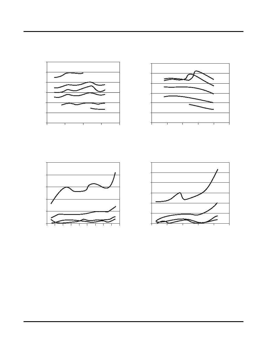
Figure 12. PLL Loop Bandwidth vs. Feedback Divider Setting (Nominal)
VCO
The ispClock5300S provides an internal VCO which provides an output frequency ranging from 160MHz to
400MHz. The VCO is implemented using differential circuit design techniques which minimize the inuence of
power supply noise on measured output jitter. The VCO is also used to generate output clock skew as a function of
the total VCO period. Using the VCO as the basis for controlling output skew allows for highly precise and consis-
tent skew generation, both from device-to-device, as well as channel-to-channel within the same device.
Output V Dividers
The ispClock5300S incorporates a set of three 5-bit programmable Power of 2 dividers which provide the ability to
synthesize output frequencies differing from that of the reference clock input.
Each one of the three V dividers can be independently programmed to provide division ratios ranging from 1 to 32
in Power of 2 steps (1, 2, 4, 8, 16, 32).
PLL Bandwidth vs.
VCO Frequency and V-Divider
(Standard Mode)
Dynamic Phase Offset vs.
Input Frequency and Modulation Index (MI)
(Vdiv = 2)
Dynamic Phase Offset vs.
Input Frequency and Modulation Index (MI)
(Vdiv = 4)
PLL Loop Bandwidth vs.
VCO Frequency and V-Divider
(Spread Spectrum Compatible Mode)
100
80
100 120 140 160 180 200 220 240 260
40
60
80
100
120
140
0.0
50
60
50
40
30
20
10
0
40
30
20
10
0
1.0
2.0
3.0
4.0
5.0
6.0
200
300
400
500
Vdiv=1
Vdiv=2
Vdiv=4
Vdiv=8
Vdiv=16
Vdiv=32
MI = 0.25%
MI = 0.50%
MI = 1.0%
MI = 2.0%
Vdiv=32
Vdiv=16
Vdiv=8
Vdiv=4
Vdiv=2
Band
width
(MHz)
VCO Frequency (MHz)
100
200
300
400
500
600
VCO Frequency (MHz)
Input Frequency (MHz)
0.0
1.0
2.0
3.0
4.0
5.0
6.0
Band
width
(MHz)
T
PDJ
(ps
RMS)
T
PDJ
(ps
RMS)
相关PDF资料 |
PDF描述 |
|---|---|
| VI-2TN-MY-F1 | CONVERTER MOD DC/DC 18.5V 50W |
| X9317WS8I-2.7T2 | IC XDCP SGL 100TAP 10K 8-SOIC |
| MS27484E24A35PC | CONN PLUG 128POS STRAIGHT W/PINS |
| SY100E154JZ TR | IC MUX-LATCH 5BIT 2:1 28PLCC |
| SY100S838LZG TR | IC CLOCK GEN 3.3V/5V 20-SOIC |
相关代理商/技术参数 |
参数描述 |
|---|---|
| ISPPACCLK5312S-01TN48C | 制造商:LATTICE 制造商全称:Lattice Semiconductor 功能描述:In-System Programmable, Zero-Delay, Universal Fan-Out Buffer, Single-Ended |
| ispPAC-CLK5312S-01TN48I | 功能描述:时钟驱动器及分配 ISP 0 Delay Unv Fan- Out Buf-Sngl End I RoHS:否 制造商:Micrel 乘法/除法因子:1:4 输出类型:Differential 最大输出频率:4.2 GHz 电源电压-最大: 电源电压-最小:5 V 最大工作温度:+ 85 C 封装 / 箱体:SOIC-8 封装:Reel |
| ISPPACCLK5312S-01TN48I | 制造商:LATTICE 制造商全称:Lattice Semiconductor 功能描述:In-System Programmable, Zero-Delay, Universal Fan-Out Buffer, Single-Ended |
| ISPPACCLK5312S-01TN64C | 制造商:LATTICE 制造商全称:Lattice Semiconductor 功能描述:In-System Programmable, Zero-Delay, Universal Fan-Out Buffer, Single-Ended |
| ISPPACCLK5312S-01TN64I | 制造商:LATTICE 制造商全称:Lattice Semiconductor 功能描述:In-System Programmable, Zero-Delay, Universal Fan-Out Buffer, Single-Ended |
发布紧急采购,3分钟左右您将得到回复。