- 您现在的位置:买卖IC网 > PDF目录9099 > ISPPAC-CLK5312S-01TN48C (Lattice Semiconductor Corporation)IC CLOCK PROGRAM BUFFER 48TQFP PDF资料下载
参数资料
| 型号: | ISPPAC-CLK5312S-01TN48C |
| 厂商: | Lattice Semiconductor Corporation |
| 文件页数: | 29/56页 |
| 文件大小: | 0K |
| 描述: | IC CLOCK PROGRAM BUFFER 48TQFP |
| 标准包装: | 250 |
| 系列: | ispClock™ |
| 类型: | 时钟发生器,扇出配送,零延迟缓冲器 |
| PLL: | 带旁路 |
| 输入: | HSTL,LVCMOS,LVDS,LVPECL,LVTTL,SSTL |
| 输出: | eHSTL,HSTL,LVCMOS,LVTTL,SSTL |
| 电路数: | 1 |
| 比率 - 输入:输出: | 2:12 |
| 差分 - 输入:输出: | 是/无 |
| 频率 - 最大: | 267MHz |
| 除法器/乘法器: | 是/无 |
| 电源电压: | 3 V ~ 3.6 V |
| 工作温度: | 0°C ~ 70°C |
| 安装类型: | 表面贴装 |
| 封装/外壳: | 48-LQFP |
| 供应商设备封装: | 48-TQFP(7x7) |
| 包装: | 托盘 |
第1页第2页第3页第4页第5页第6页第7页第8页第9页第10页第11页第12页第13页第14页第15页第16页第17页第18页第19页第20页第21页第22页第23页第24页第25页第26页第27页第28页当前第29页第30页第31页第32页第33页第34页第35页第36页第37页第38页第39页第40页第41页第42页第43页第44页第45页第46页第47页第48页第49页第50页第51页第52页第53页第54页第55页第56页
Lattice Semiconductor
ispClock5300S Family Data Sheet
35
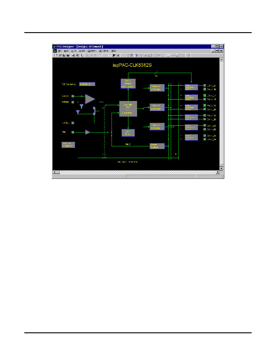
Figure 30. PAC-Designer Design Entry Screen
In-System Programming
The ispClock5300S is an In-System Programmable (ISP) device. This is accomplished by integrating all
E
2CMOS conguration control logic on-chip. Programming is performed through a 4-wire, IEEE 1149.1 compliant
serial JTAG interface at normal logic levels. Once a device is programmed, all conguration information is stored
on-chip, in non-volatile E
2CMOS memory cells. The specics of the IEEE 1149.1 serial interface and all
ispClock5300S instructions are described in the JTAG interface section of this data sheet.
User Electronic Signature
A user electronic signature (UES) feature is included in the E
2CMOS memory of the ispClock5300S. This consists
of 32 bits that can be congured by the user to store unique data such as ID codes, revision numbers or inventory
control data. The specics this feature are discussed in the IEEE 1149.1 serial interface section of this data sheet.
Electronic Security
An electronic security “fuse” (ESF) bit is provided in every ispClock5300S device to prevent unauthorized readout
of the E
2CMOS conguration bit patterns. Once programmed, this cell prevents further access to the functional
user bits in the device. This cell can only be erased by reprogramming the device, so the original conguration can
not be examined once programmed. Usage of this feature is optional. The specics of this feature are discussed in
the IEEE 1149.1 serial interface section of this data sheet.
Production Programming Support
Once a nal conguration is determined, an ASCII format JEDEC le can be created using the PAC-Designer soft-
ware. Devices can then be ordered through the usual supply channels with the user’s specic conguration already
preloaded into the devices. By virtue of its standard interface, compatibility is maintained with existing production
programming equipment, giving customers a wide degree of freedom and exibility in production planning.
相关PDF资料 |
PDF描述 |
|---|---|
| VI-2TN-MY-F1 | CONVERTER MOD DC/DC 18.5V 50W |
| X9317WS8I-2.7T2 | IC XDCP SGL 100TAP 10K 8-SOIC |
| MS27484E24A35PC | CONN PLUG 128POS STRAIGHT W/PINS |
| SY100E154JZ TR | IC MUX-LATCH 5BIT 2:1 28PLCC |
| SY100S838LZG TR | IC CLOCK GEN 3.3V/5V 20-SOIC |
相关代理商/技术参数 |
参数描述 |
|---|---|
| ISPPACCLK5312S-01TN48C | 制造商:LATTICE 制造商全称:Lattice Semiconductor 功能描述:In-System Programmable, Zero-Delay, Universal Fan-Out Buffer, Single-Ended |
| ispPAC-CLK5312S-01TN48I | 功能描述:时钟驱动器及分配 ISP 0 Delay Unv Fan- Out Buf-Sngl End I RoHS:否 制造商:Micrel 乘法/除法因子:1:4 输出类型:Differential 最大输出频率:4.2 GHz 电源电压-最大: 电源电压-最小:5 V 最大工作温度:+ 85 C 封装 / 箱体:SOIC-8 封装:Reel |
| ISPPACCLK5312S-01TN48I | 制造商:LATTICE 制造商全称:Lattice Semiconductor 功能描述:In-System Programmable, Zero-Delay, Universal Fan-Out Buffer, Single-Ended |
| ISPPACCLK5312S-01TN64C | 制造商:LATTICE 制造商全称:Lattice Semiconductor 功能描述:In-System Programmable, Zero-Delay, Universal Fan-Out Buffer, Single-Ended |
| ISPPACCLK5312S-01TN64I | 制造商:LATTICE 制造商全称:Lattice Semiconductor 功能描述:In-System Programmable, Zero-Delay, Universal Fan-Out Buffer, Single-Ended |
发布紧急采购,3分钟左右您将得到回复。