- 您现在的位置:买卖IC网 > PDF目录9099 > ISPPAC-CLK5312S-01TN48C (Lattice Semiconductor Corporation)IC CLOCK PROGRAM BUFFER 48TQFP PDF资料下载
参数资料
| 型号: | ISPPAC-CLK5312S-01TN48C |
| 厂商: | Lattice Semiconductor Corporation |
| 文件页数: | 18/56页 |
| 文件大小: | 0K |
| 描述: | IC CLOCK PROGRAM BUFFER 48TQFP |
| 标准包装: | 250 |
| 系列: | ispClock™ |
| 类型: | 时钟发生器,扇出配送,零延迟缓冲器 |
| PLL: | 带旁路 |
| 输入: | HSTL,LVCMOS,LVDS,LVPECL,LVTTL,SSTL |
| 输出: | eHSTL,HSTL,LVCMOS,LVTTL,SSTL |
| 电路数: | 1 |
| 比率 - 输入:输出: | 2:12 |
| 差分 - 输入:输出: | 是/无 |
| 频率 - 最大: | 267MHz |
| 除法器/乘法器: | 是/无 |
| 电源电压: | 3 V ~ 3.6 V |
| 工作温度: | 0°C ~ 70°C |
| 安装类型: | 表面贴装 |
| 封装/外壳: | 48-LQFP |
| 供应商设备封装: | 48-TQFP(7x7) |
| 包装: | 托盘 |
第1页第2页第3页第4页第5页第6页第7页第8页第9页第10页第11页第12页第13页第14页第15页第16页第17页当前第18页第19页第20页第21页第22页第23页第24页第25页第26页第27页第28页第29页第30页第31页第32页第33页第34页第35页第36页第37页第38页第39页第40页第41页第42页第43页第44页第45页第46页第47页第48页第49页第50页第51页第52页第53页第54页第55页第56页
Lattice Semiconductor
ispClock5300S Family Data Sheet
25
Each of the ispClock5300S’s output driver banks can be congured to support the following logic outputs:
LVTTL
LVCMOS (1.8V, 2.5V, 3.3V)
SSTL2
SSTL3
HSTL
eHSTL
To provide LVTTL, LVCMOS, SSTL2, SSTL3, HSTL and eHSTL outputs, the CMOS output drivers in each bank are
enabled. These circuits provide logic outputs which swing from ground to the VCCO supply rail. The choice of
VCCO to be supplied to a given bank is determined by the logic standard to which that bank is congured. Because
each pair of outputs has its own VCCO supply pin, each bank can be independently congured to support a differ-
ent logic standard. Note that the two outputs associated with a bank must necessarily be congured to the same
logic standard. The source impedance of each of the two outputs in each bank may be independently set over a
range of 40Ω to 70Ω in 5Ω steps. A low impedance option (≈20Ω) is also provided for cases where low source ter-
mination is desired on a given output.
Control of output slew rate is also provided in LVTTL, LVCMOS, SSTL2, SSTL3, HSTL and eHSTL output modes.
Four output slew-rate settings are provided, as specied in the “Output Rise Times” and “Output Fall Times” tables
in this data sheet.
Polarity control (true/inverted) is available for all output drivers. In the case of single-ended output standards, the
polarity of each of the two output signals from each bank may be controlled independently.
Suggested Usage
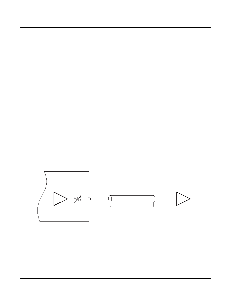
Figure 20 shows a typical conguration for the ispClock5300S output driver when congured to drive an LVTTL or
LVCMOS load. The ispClock5300S output impedance should be set to match the characteristic impedance of the
transmission line being driven. The far end of the transmission line should be left open, with no termination resis-
tors.
Figure 20. Conguration for LVTTL/LVCMOS Output Modes
Figure 21 shows a typical conguration for the ispClock5300S output driver when congured to drive SSTL2,
SSTL3, HSTL or eHSTL loads. The ispClock5300S output impedance should be set to 40Ω for driving SSTL2 or
SSTL3 loads and to the ≈20Ω setting for driving HSTL and eHSTL. The far end of the transmission line must be ter-
minated to an appropriate VTT voltage through a 50Ω resistor.
Zo
Ro = Zo
ispClock5300S
LVCMOS/LVTTL
Mode
LVCMOS/LVTTL
Receiver
相关PDF资料 |
PDF描述 |
|---|---|
| VI-2TN-MY-F1 | CONVERTER MOD DC/DC 18.5V 50W |
| X9317WS8I-2.7T2 | IC XDCP SGL 100TAP 10K 8-SOIC |
| MS27484E24A35PC | CONN PLUG 128POS STRAIGHT W/PINS |
| SY100E154JZ TR | IC MUX-LATCH 5BIT 2:1 28PLCC |
| SY100S838LZG TR | IC CLOCK GEN 3.3V/5V 20-SOIC |
相关代理商/技术参数 |
参数描述 |
|---|---|
| ISPPACCLK5312S-01TN48C | 制造商:LATTICE 制造商全称:Lattice Semiconductor 功能描述:In-System Programmable, Zero-Delay, Universal Fan-Out Buffer, Single-Ended |
| ispPAC-CLK5312S-01TN48I | 功能描述:时钟驱动器及分配 ISP 0 Delay Unv Fan- Out Buf-Sngl End I RoHS:否 制造商:Micrel 乘法/除法因子:1:4 输出类型:Differential 最大输出频率:4.2 GHz 电源电压-最大: 电源电压-最小:5 V 最大工作温度:+ 85 C 封装 / 箱体:SOIC-8 封装:Reel |
| ISPPACCLK5312S-01TN48I | 制造商:LATTICE 制造商全称:Lattice Semiconductor 功能描述:In-System Programmable, Zero-Delay, Universal Fan-Out Buffer, Single-Ended |
| ISPPACCLK5312S-01TN64C | 制造商:LATTICE 制造商全称:Lattice Semiconductor 功能描述:In-System Programmable, Zero-Delay, Universal Fan-Out Buffer, Single-Ended |
| ISPPACCLK5312S-01TN64I | 制造商:LATTICE 制造商全称:Lattice Semiconductor 功能描述:In-System Programmable, Zero-Delay, Universal Fan-Out Buffer, Single-Ended |
发布紧急采购,3分钟左右您将得到回复。