- 您现在的位置:买卖IC网 > PDF目录9099 > ISPPAC-CLK5312S-01TN48C (Lattice Semiconductor Corporation)IC CLOCK PROGRAM BUFFER 48TQFP PDF资料下载
参数资料
| 型号: | ISPPAC-CLK5312S-01TN48C |
| 厂商: | Lattice Semiconductor Corporation |
| 文件页数: | 12/56页 |
| 文件大小: | 0K |
| 描述: | IC CLOCK PROGRAM BUFFER 48TQFP |
| 标准包装: | 250 |
| 系列: | ispClock™ |
| 类型: | 时钟发生器,扇出配送,零延迟缓冲器 |
| PLL: | 带旁路 |
| 输入: | HSTL,LVCMOS,LVDS,LVPECL,LVTTL,SSTL |
| 输出: | eHSTL,HSTL,LVCMOS,LVTTL,SSTL |
| 电路数: | 1 |
| 比率 - 输入:输出: | 2:12 |
| 差分 - 输入:输出: | 是/无 |
| 频率 - 最大: | 267MHz |
| 除法器/乘法器: | 是/无 |
| 电源电压: | 3 V ~ 3.6 V |
| 工作温度: | 0°C ~ 70°C |
| 安装类型: | 表面贴装 |
| 封装/外壳: | 48-LQFP |
| 供应商设备封装: | 48-TQFP(7x7) |
| 包装: | 托盘 |
第1页第2页第3页第4页第5页第6页第7页第8页第9页第10页第11页当前第12页第13页第14页第15页第16页第17页第18页第19页第20页第21页第22页第23页第24页第25页第26页第27页第28页第29页第30页第31页第32页第33页第34页第35页第36页第37页第38页第39页第40页第41页第42页第43页第44页第45页第46页第47页第48页第49页第50页第51页第52页第53页第54页第55页第56页
Lattice Semiconductor
ispClock5300S Family Data Sheet
2
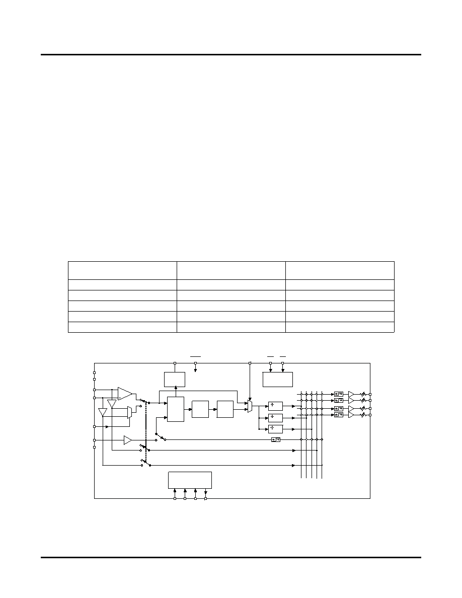
General Description
The ispClock5300S is an in-system-programmable zero delay universal fan-out buffer for use in clock distribution
applications. The ispClock5312S, the rst member of the ispClock5300S family, provides up to 12 single-ended
ultra low skew outputs. Each pair of outputs may be independently congured to support separate I/O standards
(LVTTL, LVCMOS -3.3V, 2.5V, 1.8, SSTL, HSTL) and output frequency. In addition, each output provides indepen-
dent programmable control of termination, slew-rate, and timing skew. All conguration information is stored on-
chip in non-volatile E
2CMOS memory.
The ispClock5300S devices provide extremely low propagation delay (zero-delay) from input to output using the
on-chip low jitter high-performance PLL. A set of three programmable 5-bit counters can be used to generate three
frequencies derived from the PLL clock. These counters are programmable in powers of 2 only (1, 2, 4, 8, 16, 32).
The clock output from any of the V-dividers can then be routed to any clock output pin through the output routing
matrix. The output routing matrix, in addition, also enables routing of reference clock inputs directly to any output.
The ispClock5300S device can be congured to operate in four modes: zero delay buffer mode, dual non-zero
delay buffer mode, non-zero delay buffer mode with output dividers, and combined zero-delay and non-zero delay
buffer mode.
The core functions of all members of the ispClock5300S family are identical. Table 1 summarizes the
ispClock5300S device family.
Table 1. ispClock5300S Family
Figure 1. ispClock5304S Functional Block Diagram
Device
Number of Programmable
Clock Inputs
Number of Programmable
Single-Ended Outputs
ispClock5320S
1 Differential, 2 Single-Ended
20
ispClock5316S
1 Differential, 2 Single-Ended
16
ispClock5312S
1 Differential, 2 Single-Ended
12
ispClock5308S
1 Differential, 2 Single-Ended
8
ispClock5304S
1 Differential, 2 Single-Ended
4
+
VCO
LOOP
FILTER
PHASE
DETECT
LOCK
DETECT
REFA_REFP
REFSEL
VTT_REFB
1
0
OEX
S
A
P
Y
B
_
L
P
K
C
O
L
JTAG INTERFACE
OEY
TDO
TCK
TMS
TDI
SKEW
CONTROL
OUTPUT
DRIVERS
SKEW
CONTROL
OUTPUT
DRIVERS
OUTPUT
DIVIDERS
OUTPUT ROUTING
MATRIX
RESET
V1
V2
V0
BANK_0A
BANK_0B
BANK_1A
BANK_1B
OUTPUT ENABLE
CONTROLS
5-bit
0
1
FBK
REFB_REFN
VTT_REFA
VTT_FBK
相关PDF资料 |
PDF描述 |
|---|---|
| VI-2TN-MY-F1 | CONVERTER MOD DC/DC 18.5V 50W |
| X9317WS8I-2.7T2 | IC XDCP SGL 100TAP 10K 8-SOIC |
| MS27484E24A35PC | CONN PLUG 128POS STRAIGHT W/PINS |
| SY100E154JZ TR | IC MUX-LATCH 5BIT 2:1 28PLCC |
| SY100S838LZG TR | IC CLOCK GEN 3.3V/5V 20-SOIC |
相关代理商/技术参数 |
参数描述 |
|---|---|
| ISPPACCLK5312S-01TN48C | 制造商:LATTICE 制造商全称:Lattice Semiconductor 功能描述:In-System Programmable, Zero-Delay, Universal Fan-Out Buffer, Single-Ended |
| ispPAC-CLK5312S-01TN48I | 功能描述:时钟驱动器及分配 ISP 0 Delay Unv Fan- Out Buf-Sngl End I RoHS:否 制造商:Micrel 乘法/除法因子:1:4 输出类型:Differential 最大输出频率:4.2 GHz 电源电压-最大: 电源电压-最小:5 V 最大工作温度:+ 85 C 封装 / 箱体:SOIC-8 封装:Reel |
| ISPPACCLK5312S-01TN48I | 制造商:LATTICE 制造商全称:Lattice Semiconductor 功能描述:In-System Programmable, Zero-Delay, Universal Fan-Out Buffer, Single-Ended |
| ISPPACCLK5312S-01TN64C | 制造商:LATTICE 制造商全称:Lattice Semiconductor 功能描述:In-System Programmable, Zero-Delay, Universal Fan-Out Buffer, Single-Ended |
| ISPPACCLK5312S-01TN64I | 制造商:LATTICE 制造商全称:Lattice Semiconductor 功能描述:In-System Programmable, Zero-Delay, Universal Fan-Out Buffer, Single-Ended |
发布紧急采购,3分钟左右您将得到回复。