- 您现在的位置:买卖IC网 > PDF目录9099 > ISPPAC-CLK5312S-01TN48C (Lattice Semiconductor Corporation)IC CLOCK PROGRAM BUFFER 48TQFP PDF资料下载
参数资料
| 型号: | ISPPAC-CLK5312S-01TN48C |
| 厂商: | Lattice Semiconductor Corporation |
| 文件页数: | 55/56页 |
| 文件大小: | 0K |
| 描述: | IC CLOCK PROGRAM BUFFER 48TQFP |
| 标准包装: | 250 |
| 系列: | ispClock™ |
| 类型: | 时钟发生器,扇出配送,零延迟缓冲器 |
| PLL: | 带旁路 |
| 输入: | HSTL,LVCMOS,LVDS,LVPECL,LVTTL,SSTL |
| 输出: | eHSTL,HSTL,LVCMOS,LVTTL,SSTL |
| 电路数: | 1 |
| 比率 - 输入:输出: | 2:12 |
| 差分 - 输入:输出: | 是/无 |
| 频率 - 最大: | 267MHz |
| 除法器/乘法器: | 是/无 |
| 电源电压: | 3 V ~ 3.6 V |
| 工作温度: | 0°C ~ 70°C |
| 安装类型: | 表面贴装 |
| 封装/外壳: | 48-LQFP |
| 供应商设备封装: | 48-TQFP(7x7) |
| 包装: | 托盘 |
第1页第2页第3页第4页第5页第6页第7页第8页第9页第10页第11页第12页第13页第14页第15页第16页第17页第18页第19页第20页第21页第22页第23页第24页第25页第26页第27页第28页第29页第30页第31页第32页第33页第34页第35页第36页第37页第38页第39页第40页第41页第42页第43页第44页第45页第46页第47页第48页第49页第50页第51页第52页第53页第54页当前第55页第56页
Lattice Semiconductor
ispClock5300S Family Data Sheet
8
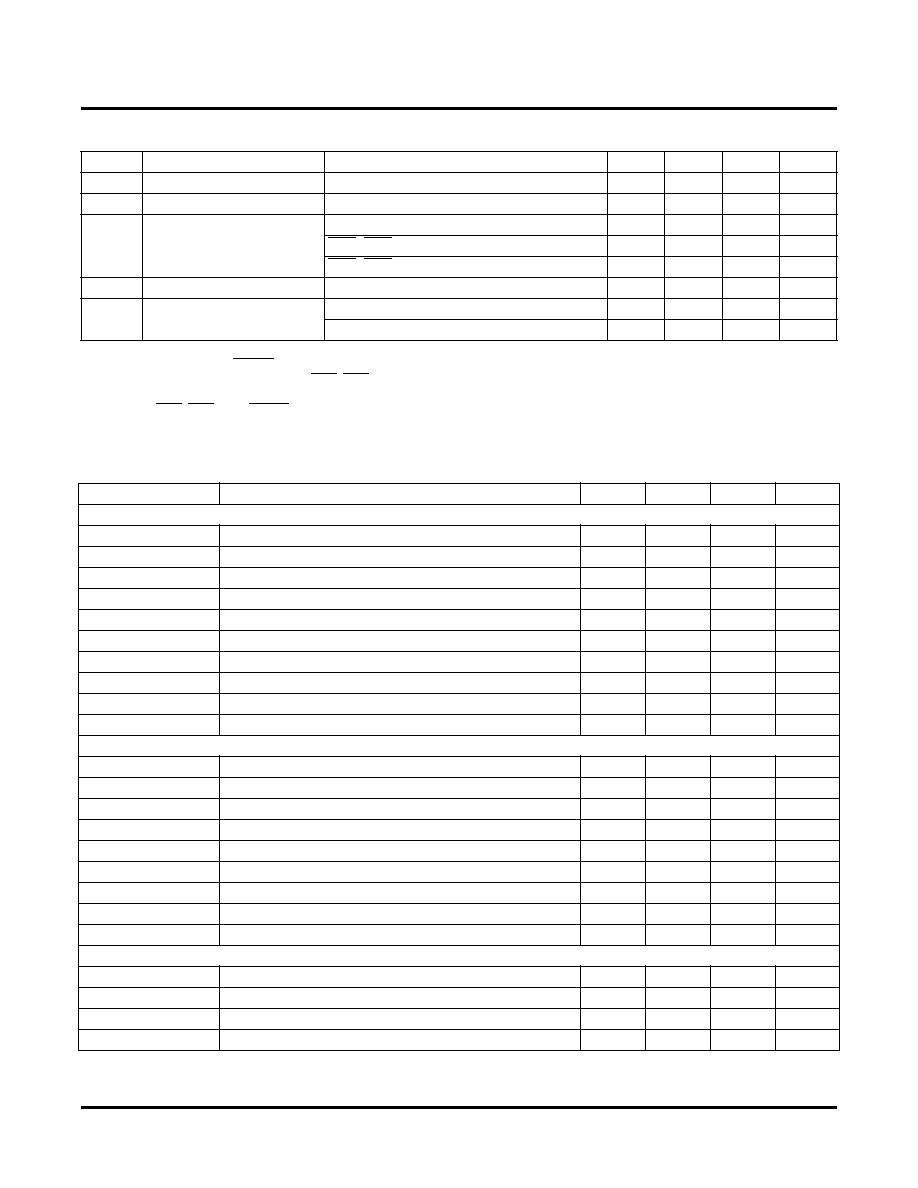
DC Electrical Characteristics – Input/Output Loading
Switching Characteristics – Timing Adders for I/O Modes
Symbol
Parameter
Conditions
Min.
Typ.
Max.
Units
ILK
Input Leakage
Note 1
—
±10
A
IPU
Input Pull-up Current
Note 2
—
80
120
A
IPD
Input Pull-down Current
REFSEL, PLL_BYPASS
—
120
150
A
OEX, OEY, 2.5V CMOS Logic Standard
—
120
150
A
OEX, OEY, & 3.3V CMOS Logic Standard
—
200
400
A
IOLK
Tristate Leakage Output
Note 4
—
±10
A
CIN
Input Capacitance
Notes 2, 3, 5
—
8
10
pF
Note 6
—
10
11
pF
1. Applies to clock reference inputs when termination ‘open’.
2. Applies to TDI, TMS and RESET inputs.
3. Applies to REFSEL and PLL_BYPASS, OEX, OEY.
4. Applies to all logic types when in tristated mode.
5. Applies to OEX, OEY, TCK, RESET inputs.
6. Applies to REFA_REFP, REFB_REFN, FBK.
Adder Type
Description
Min.
Typ.
Max.
Units
tIOI Input Adders
2
LVTTL_in
Using LVTTL Standard
0.00
ns
LVCMOS18_in
Using LVCMOS 1.8V Standard
0.10
ns
LVCMOS25_in
Using LVCMOS 2.5V Standard
0.00
ns
LVCMOS33_in
Using LVCMOS 3.3V Standard
0.00
ns
SSTL2_in
Using SSTL2 Standard
0.00
ns
SSTL3_in
Using SSTL3 Standard
0.00
ns
HSTL_in
Using HSTL Standard
1.15
ns
eHSTL_in
Using eHSTL Standard
1.10
ns
LVDS_in
Using LVDS Standard
0.60
ns
LVPECL_in
Using LVPECL Standard
0.60
ns
tIOO Output Adders
1, 3
LVTTL_out
Output Congured as LVTTL Buffer
0.25
ns
LVCMOS18_out
Output Congured as LVCMOS 1.8V Buffer
0.25
ns
LVCMOS25_out
Output Congured as LVCMOS 2.5V Buffer
0.25
ns
LVCMOS33_out
Output Congured as LVCMOS 3.3V Buffer
0.25
ns
SSTL18_out
Output Congured as SSTL18 Buffer
0.00
ns
SSTL2_out
Output Congured as SSTL2 Buffer
0.00
ns
SSTL3_out
Output Congured as SSTL3 Buffer
0.00
ns
HSTL_out
Output Congured as HSTL Buffer
0.00
ns
eHSTL_out
Output Congured as eHSTL Buffer
0.00
ns
tIOS Output Slew Rate Adders
1
Slew_1
Output Slew_1 (Fastest)
—
0.00
—
ps
Slew_2
Output Slew_2
—
475
—
ps
Slew_3
Output Slew_3
—
950
—
ps
Slew_4
Output Slew_4 (Slowest)
—
1900
—
ps
2. All input adders referenced to LVTTL.
3. All output adders referenced to SSTL/HSTL/eHSTL.
相关PDF资料 |
PDF描述 |
|---|---|
| VI-2TN-MY-F1 | CONVERTER MOD DC/DC 18.5V 50W |
| X9317WS8I-2.7T2 | IC XDCP SGL 100TAP 10K 8-SOIC |
| MS27484E24A35PC | CONN PLUG 128POS STRAIGHT W/PINS |
| SY100E154JZ TR | IC MUX-LATCH 5BIT 2:1 28PLCC |
| SY100S838LZG TR | IC CLOCK GEN 3.3V/5V 20-SOIC |
相关代理商/技术参数 |
参数描述 |
|---|---|
| ISPPACCLK5312S-01TN48C | 制造商:LATTICE 制造商全称:Lattice Semiconductor 功能描述:In-System Programmable, Zero-Delay, Universal Fan-Out Buffer, Single-Ended |
| ispPAC-CLK5312S-01TN48I | 功能描述:时钟驱动器及分配 ISP 0 Delay Unv Fan- Out Buf-Sngl End I RoHS:否 制造商:Micrel 乘法/除法因子:1:4 输出类型:Differential 最大输出频率:4.2 GHz 电源电压-最大: 电源电压-最小:5 V 最大工作温度:+ 85 C 封装 / 箱体:SOIC-8 封装:Reel |
| ISPPACCLK5312S-01TN48I | 制造商:LATTICE 制造商全称:Lattice Semiconductor 功能描述:In-System Programmable, Zero-Delay, Universal Fan-Out Buffer, Single-Ended |
| ISPPACCLK5312S-01TN64C | 制造商:LATTICE 制造商全称:Lattice Semiconductor 功能描述:In-System Programmable, Zero-Delay, Universal Fan-Out Buffer, Single-Ended |
| ISPPACCLK5312S-01TN64I | 制造商:LATTICE 制造商全称:Lattice Semiconductor 功能描述:In-System Programmable, Zero-Delay, Universal Fan-Out Buffer, Single-Ended |
发布紧急采购,3分钟左右您将得到回复。