- 您现在的位置:买卖IC网 > PDF目录20492 > IXDN430MYI (IXYS)IC MOSFET/IGBT DRIVER TO-263 PDF资料下载
参数资料
| 型号: | IXDN430MYI |
| 厂商: | IXYS |
| 文件页数: | 12/12页 |
| 文件大小: | 0K |
| 描述: | IC MOSFET/IGBT DRIVER TO-263 |
| 标准包装: | 50 |
| 配置: | 低端 |
| 输入类型: | 非反相 |
| 延迟时间: | 41ns |
| 电流 - 峰: | 30A |
| 配置数: | 1 |
| 输出数: | 1 |
| 电源电压: | 8.5 V ~ 35 V |
| 工作温度: | -55°C ~ 125°C |
| 安装类型: | 表面贴装 |
| 封装/外壳: | TO-263-6,D²Pak(5 引线+接片),TO-263BA |
| 供应商设备封装: | TO-263 |
| 包装: | 盒 |
| 配用: | EVDN430MYI-ND - BOARD EVALUATION IXDN430MYI |
| 其它名称: | Q1952551 |
�� �
�
�IXDN430� /� IXDI430� /� IXDD430� /� IXDS430�
�OUTPUT LEAD INDUCTANCE�
�Of� equal� importance� to� Supply� Bypassing� and� Grounding� are�
�issues� related� to� the� Output� Lead� Inductance.� Every� effort�
�should� be� made� to� keep� the� leads� between� the� driver� and� it’s�
�load� as� short� and� wide� as� possible.� If� the� driver� must� be� placed�
�farther� than� 2”� from� the� load,� then� the� output� leads� should� be�
�treated� as� transmission� lines.� In� this� case,� a� twisted-pair�
�should� be� considered,� and� the� return� line� of� each� twisted� pair�
�should� be� placed� as� close� as� possible� to� the� ground� pin� of� the�
�driver,� and� connect� directly� to� the� ground� terminal� of� the� load.�
�TTL to High Voltage CMOS Level Translation�
�(IXDD430 Only)�
�The� enable� (EN)� input� to� the� IXDD430� is� a� high� voltage�
�CMOS� logic� level� input� where� the� EN� input� threshold� is� ?�
�V� CC� ,� and� may� not� be� compatible� with� 5V� CMOS� or� TTL� input�
�levels.� The� IXDD430� EN� input� was� intentionally� designed�
�for� enhanced� noise� immunity� with� the� high� voltage� CMOS�
�logic� levels.� In� a� typical� gate� driver� application,� V� CC� =15V�
�and� the� EN� input� threshold� at� 7.5V,� a� 5V� CMOS� logical� high�
�input� applied� to� this� typical� IXDD430� application’s� EN� input�
�A� TTL� or� 5V� CMOS� logic� low,� V� TTLLOW� =~<0.8V,� input� applied� to� the�
�Q1� emitter� will� drive� it� on.� This� causes� the� level� translator�
�output,� the� Q1� collector� output� to� settle� to� V� CESATQ1� +�
�V� TTLLOW� =<~2V,� which� is� sufficiently� low� to� be� correctly� interpreted�
�as� a� high� voltage� CMOS� logic� low� (<1/3V� CC� =5V� for� V� CC� =15V� given�
�in� the� IXDD430� data� sheet.)�
�A� TTL� high,� V� TTLHIGH� =>~2.4V,� or� a� 5V� CMOS� high,�
�V� 5VCMOSHIGH� =~>3.5V,� applied� to� the� EN� input� of� the� circuit� in�
�Figure� 29� will� cause� Q1� to� be� biased� off.� This� results� in� Q1�
�collector� being� pulled� up� by� R3� to� V� CC� =15V,� and� provides� a�
�high� voltage� CMOS� logic� high� output.� The� high� voltage� CMOS�
�logical� EN� output� applied� to� the� IXDD430� EN� input� will� enable�
�it,� allowing� the� gate� driver� to� fully� function� as� an� 30� Amp�
�output� driver.�
�The� total� component� cost� of� the� circuit� in� Figure� 29� is� less�
�than� $0.10� if� purchased� in� quantities� >1K� pieces.� It� is�
�recommended� that� the� physical� placement� of� the� level�
�translator� circuit� be� placed� close� to� the� source� of� the� TTL� or�
�CMOS� logic� circuits� to� maximize� noise� rejection.�
�will� be� misinterpreted� as� a� logical� low,� and� may� cause�
�undesirable� or� unexpected� results.� The� note� below� is� for�
�optional� adaptation� of� TTL� or� 5V� CMOS� levels.�
�The� circuit� in� Figure� 29� alleviates� this� potential� logic� level�
�misinterpretation� by� translating� a� TTL� or� 5V� CMOS� logic�
�input� to� high� voltage� CMOS� logic� levels� needed� by� the�
�IXDD430� EN� input.� From� the� figure,� V� CC� is� the� gate� driver�
�power� supply,� typically� set� between� 8V� to� 20V,� and� V� DD� is�
�the� logic� power� supply,� typically� between� 3.3V� to� 5.5V.�
�Resistors� R1� and� R2� form� a� voltage� divider� network� so�
�that� the� Q1� base� is� positioned� at� the� midpoint� of� the�
�expected� TTL� logic� transition� levels.�
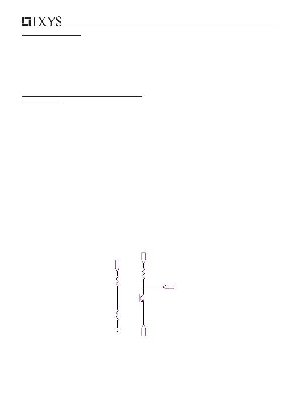
�Figure� 29� -� TTL� to� High� Voltage� CMOS� Level� Translator�
�Vcc�
�(From� gate� driver�
�power� supply)�
�(From� logic�
�Vdd�
�power� supply)�
�R3�
�10K�
�R1�
�10K�
�Q1�
�High� Voltage�
�CMOS� EN� output�
�(To� IXDD430� EN� input)�
�2N3904�
�R2�
�10K�
�5V� CMOS� or� TTL� input�
�EN�
�IXYS� Corporation�
�3540� Bassett� St;� Santa� Clara,� CA� 95054�
�Tel:� 408-982-0700;� Fax:� 408-496-0670�
�www.ixys.com�
�e-mail:� sales@ixys.net�
�12�
�IXYS� Semiconductor� GmbH�
�Edisonstrasse15� ;� D-68623;� Lampertheim�
�Tel:� +49-6206-503-0;� Fax:� +49-6206-503627�
�e-mail:� marcom@ixys.de�
�DS99045A(8/03)�
�相关PDF资料 |
PDF描述 |
|---|---|
| RBB06DHRD | CONN CARD EXTEND 12POS .050" |
| VE-2N2-CX-S | CONVERTER MOD DC/DC 15V 75W |
| RKZ-0505D/H | CONV DC/DC 2W 05VIN +/-05VOUT |
| VE-2NJ-CX-S | CONVERTER MOD DC/DC 36V 75W |
| VE-2NH-CX-S | CONVERTER MOD DC/DC 52V 75W |
相关代理商/技术参数 |
参数描述 |
|---|---|
| IXDN430YI | 功能描述:功率驱动器IC 30 Amps 40V 0.4 Rds RoHS:否 制造商:Micrel 产品:MOSFET Gate Drivers 类型:Low Cost High or Low Side MOSFET Driver 上升时间: 下降时间: 电源电压-最大:30 V 电源电压-最小:2.75 V 电源电流: 最大功率耗散: 最大工作温度:+ 85 C 安装风格:SMD/SMT 封装 / 箱体:SOIC-8 封装:Tube |
| IXDN502D1 | 功能描述:功率驱动器IC 2 Amps 35V 3 Rds RoHS:否 制造商:Micrel 产品:MOSFET Gate Drivers 类型:Low Cost High or Low Side MOSFET Driver 上升时间: 下降时间: 电源电压-最大:30 V 电源电压-最小:2.75 V 电源电流: 最大功率耗散: 最大工作温度:+ 85 C 安装风格:SMD/SMT 封装 / 箱体:SOIC-8 封装:Tube |
| IXDN502D1T/R | 功能描述:功率驱动器IC 40V 4A RoHS:否 制造商:Micrel 产品:MOSFET Gate Drivers 类型:Low Cost High or Low Side MOSFET Driver 上升时间: 下降时间: 电源电压-最大:30 V 电源电压-最小:2.75 V 电源电流: 最大功率耗散: 最大工作温度:+ 85 C 安装风格:SMD/SMT 封装 / 箱体:SOIC-8 封装:Tube |
| IXDN502PI | 功能描述:功率驱动器IC 40V 4A RoHS:否 制造商:Micrel 产品:MOSFET Gate Drivers 类型:Low Cost High or Low Side MOSFET Driver 上升时间: 下降时间: 电源电压-最大:30 V 电源电压-最小:2.75 V 电源电流: 最大功率耗散: 最大工作温度:+ 85 C 安装风格:SMD/SMT 封装 / 箱体:SOIC-8 封装:Tube |
| IXDN502SIA | 功能描述:功率驱动器IC 2 Amps 40V 3.0 Ohms Rds RoHS:否 制造商:Micrel 产品:MOSFET Gate Drivers 类型:Low Cost High or Low Side MOSFET Driver 上升时间: 下降时间: 电源电压-最大:30 V 电源电压-最小:2.75 V 电源电流: 最大功率耗散: 最大工作温度:+ 85 C 安装风格:SMD/SMT 封装 / 箱体:SOIC-8 封装:Tube |
发布紧急采购,3分钟左右您将得到回复。