- 您现在的位置:买卖IC网 > PDF目录1223 > KIT33996EKEVB (Freescale Semiconductor)KIT EVAL 33996 16OUTPUT SW W/SPI PDF资料下载
参数资料
| 型号: | KIT33996EKEVB |
| 厂商: | Freescale Semiconductor |
| 文件页数: | 16/24页 |
| 文件大小: | 0K |
| 描述: | KIT EVAL 33996 16OUTPUT SW W/SPI |
| 标准包装: | 1 |
| 主要目的: | 电源管理,低端驱动器(内部 FET) |
| 嵌入式: | 否 |
| 已用 IC / 零件: | MC33996 |
| 主要属性: | 16 输出,5 ~ 27V,0.9 ~ 2.5A,SPI 接口,PWM 接口 |
| 次要属性: | 0.55 欧 RdsON,温度,过压,短路保护 |
| 已供物品: | 板,CD |
| 相关产品: | MC33996EK-ND - IC SWITCH 16OUTPUT W/SPI 32-SOIC MC33996EKR2-ND - IC SWITCH 16-OTPT W/SPI 32-SOIC |
�� �
�
�TYPICAL� APPLICATIONS�
�INTRODUCTION�
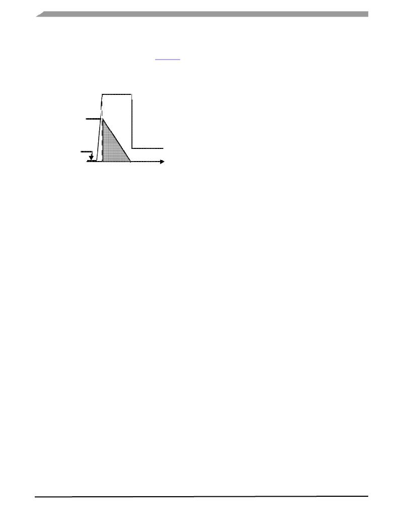
�calculated� by� multiplying� the� current� area� under� the� current�
�curve� (I� A� )� times� the� clamp� voltage� (V� CL� )� (see� Figure� 13� ).�
�Characterization� of� the� output� clamps,� using� a� single� pulse�
�non-repetitive� method� at� 0.3A,� indicates� the� maximum�
�energy� to� be� 50mJ� at� 150� °� C� junction� temperature� per� output.�
�Drain-to-Source� C� lamp�
�=� Voltage� (V� CL� 45� V)� 50� V)�
�Drain-to-Source� C� lamp� Drain� Voltage�
�Voltage� (V� CL� =� 50V)�
�All� outputs� consist� of� a� power� MOSFET� with� an� integral�
�substrate� diode.� During� reverse� battery� condition,� current� will�
�flow� through� the� load� via� the� substrate� diode.� Under� this�
�circumstance� relays� may� energize� and� lamps� will� turn� on.� If�
�load� reverse� battery� protection� is� desired,� a� diode� must� be�
�placed� in� series� with� the� load.�
�Over-temperature� Fault�
�(I� (I� D� D� =� 0.3A)� A)�
�Clamp� Energy�
�(E� (E� I� AVG� x� V� CL� )�
�Drain� Current�
�=� 0.3�
�Clamp� Energy�
�J� A� CL�
�Over-temperature� detect� circuits� are� specifically�
�incorporated� for� each� individual� output.� The� shutdown�
�following� an� over� temperature� condition� depends� on� the�
�control� bit� set� in� the� Global� Shutdown� /� Retry� Control� register.�
�Each� independent� output� shuts� down� at� 155°C� to� 180°C.�
�Voltage� (V� DS� (O� N)� )� )�
�G� ND�
�Drain-to-Source� ON�
�Voltage� (V�
�DS(ON)�
�GND�
�Curren� t�
�Area� (I� A� )�
�Time�
�When� an� output� shuts� down� due� to� an� Over-temperature�
�Fault,� no� other� outputs� are� affected.� The� MCU� recognizes� the�
�fault� by� a� logic� [1]� in� the� Fault� Status� bit� (bit� 23� in� the� SO�
�Response� register).� After� the� 33996� has� cooled� below� the�
�Figure� 13.� Output� Voltage� Clamping�
�Reverse� Battery� Protection�
�switch� point� temperature� and� 10°C� hysteresis,� the� output� will�
�function� as� defined� by� the� shutdown� /� retry� bit� 17� in� the� Global�
�Shutdown/Retry� Control� register.�
�The� 33996� device� requires� external� reverse� battery�
�protection� on� the� VPWR� pin.�
�33996�
�Analog� Integrated� Circuit� Device� Data�
�16�
�Freescale� Semiconductor�
�相关PDF资料 |
PDF描述 |
|---|---|
| KIT34673EPEVBE | KIT EVALUATION FOR MC34673 |
| KIT34674EPEVBE | KIT EVAL BOARD 10CH LED BACKLGHT |
| KIT34675EPEVBE | KIT EVALUATION FOR MC34675 |
| KIT35XS3500EVBE | KIT EVAL QUAD HIGH SIDE SWITCH |
| KITUSBSPIEVME | KIT EVAL USB-SPI W/MC68HC908JW32 |
相关代理商/技术参数 |
参数描述 |
|---|---|
| KIT33999EKEVB | 功能描述:电源管理IC开发工具 33999 PDOSS EVAL KIT RoHS:否 制造商:Maxim Integrated 产品:Evaluation Kits 类型:Battery Management 工具用于评估:MAX17710GB 输入电压: 输出电压:1.8 V |
| KIT34670EGEVBE | 功能描述:电源管理IC开发工具 IEEE 802.3AF PD WITH CUR RoHS:否 制造商:Maxim Integrated 产品:Evaluation Kits 类型:Battery Management 工具用于评估:MAX17710GB 输入电压: 输出电压:1.8 V |
| KIT34671EPEVBE | 功能描述:电源管理IC开发工具 HIGH-INPUT-VOLT CHARGER RoHS:否 制造商:Maxim Integrated 产品:Evaluation Kits 类型:Battery Management 工具用于评估:MAX17710GB 输入电压: 输出电压:1.8 V |
| KIT34673EPEVBE | 功能描述:电源管理IC开发工具 IC, HIGH-INPUT-VOLT CHARGER RoHS:否 制造商:Maxim Integrated 产品:Evaluation Kits 类型:Battery Management 工具用于评估:MAX17710GB 输入电压: 输出电压:1.8 V |
| KIT34674EPEVBE | 功能描述:电源管理IC开发工具 IC, 10 CH LED BACKLIGHT RoHS:否 制造商:Maxim Integrated 产品:Evaluation Kits 类型:Battery Management 工具用于评估:MAX17710GB 输入电压: 输出电压:1.8 V |
发布紧急采购,3分钟左右您将得到回复。