- 您现在的位置:买卖IC网 > PDF目录79959 > L6919ETR (STMICROELECTRONICS) SWITCHING CONTROLLER, PDSO28 PDF资料下载
参数资料
| 型号: | L6919ETR |
| 厂商: | STMICROELECTRONICS |
| 元件分类: | 稳压器 |
| 英文描述: | SWITCHING CONTROLLER, PDSO28 |
| 封装: | SO-28 |
| 文件页数: | 16/33页 |
| 文件大小: | 644K |
| 代理商: | L6919ETR |
第1页第2页第3页第4页第5页第6页第7页第8页第9页第10页第11页第12页第13页第14页第15页当前第16页第17页第18页第19页第20页第21页第22页第23页第24页第25页第26页第27页第28页第29页第30页第31页第32页第33页
Obsolete
Product(s)
- Obsolete
Product(s)
23/33
L6919E
– An additional 100nF ceramic capacitor is suggested to place near HS mosfet drain. This helps in reduc-
ing noise.
– PHASE pin spikes. Since the HS mosfet switches in hard mode, heavy voltage spikes can be observed
on the PHASE pins. If these voltage spikes overcome the max breakdown voltage of the pin, the device
can absorb energy and it can cause damages. The voltage spikes must be limited by proper layout, the
use of gate resistors, Schottky diodes in parallel to the low side mosfets and/or snubber network on the
low side mosfets, to a value lower than 26V, for 20nSec, at FSW of 600kHz max.
s
Current Sense Connections.
Remote Buffer: The input connections for this components must be routed as parallel nets from the FBG/FBR
pins to the load in order to compensate losses along the output power traces and also to avoid the pick-up of
any common mode noise. Connecting these pins in points far from the load, will cause a non-optimum load reg-
ulation, increasing output tolerance.
Current Reading: The Rg resistor has to be placed as close as possible to the ISENx and PGNDSx pins in
order to limit the noise injection into the device. The PCB traces connecting these resistors to the reading point
must be routed as parallel traces in order to avoid the pick-up of any common mode noise. It's also important
to avoid any offset in the measurement and to get a better precision, to connect the traces as close as possible
to the sensing elements, dedicated current sense resistor or low side mosfet RdsON.
Moreover, when using the low side mosfet RdsON as current sense element, the ISENx pin is practically con-
nected to the PHASEx pin. DO NOT CONNECT THE PINS TOGETHER AND THEN TO THE HS SOURCE!
The device won't work properly because of the noise generated by the return of the high side driver. In this case
route two separate nets: connect the PHASEx pin to the HS Source (route together with HGATEx) with a wide
net (30 mils) and the ISENx pin to the LS Drain (route together with PGNDSx). Moreover, the PGNDSx pin is
always connected, through the Rg resistor, to the PGND: DO NOT CONNECT DIRECTLY TO THE PGND! In
this case the device won't work properly. Route anyway to the LS mosfet source (together with ISENx net).
Right and wrong connections are reported in Figure 18.
Symmetrical layout is also suggested to avoid any unbalance between the two phases of the converter.
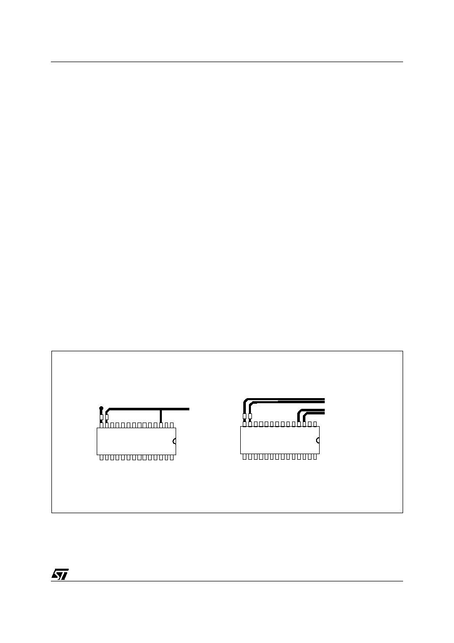
Figure 18. PCB layout connections for sense nets
Wrong (left) and correct (right) connections for the current reading sensing nets.
NOT CORRECT
CORRECT
To PHASE
connection
VIA to GND plane
To HS Gate
and Source
To LS Drain
and Source
相关PDF资料 |
PDF描述 |
|---|---|
| LUW025F8 | 1-OUTPUT 16.5 W DC-DC REG PWR SUPPLY MODULE |
| L5973ADTR | 2.3 A SWITCHING REGULATOR, PDSO8 |
| LSN-1.8/10-D12BH | DC-DC REG PWR SUPPLY MODULE |
| LM2575-33IN | 4 A SWITCHING REGULATOR, 63 kHz SWITCHING FREQ-MAX, PDIP16 |
| LM2575IKTT | 4 A SWITCHING REGULATOR, 63 kHz SWITCHING FREQ-MAX, PSSO5 |
相关代理商/技术参数 |
参数描述 |
|---|---|
| L-692 | 制造商:RHOMBUS-IND 制造商全称:Rhombus Industries Inc. 功能描述:Common Mode Inductor |
| L6920 | 制造商:STMICROELECTRONICS 制造商全称:STMicroelectronics 功能描述:1V HIGH EFFICIENCY SYNCRONOUS STEP UP CONVERTER |
| L6920D | 功能描述:直流/直流开关转换器 0.6 to 5.5V Step-Up RoHS:否 制造商:STMicroelectronics 最大输入电压:4.5 V 开关频率:1.5 MHz 输出电压:4.6 V 输出电流:250 mA 输出端数量:2 最大工作温度:+ 85 C 安装风格:SMD/SMT |
| L6920DB | 功能描述:直流/直流开关转换器 Synchronous Rectifer Step Up Converter RoHS:否 制造商:STMicroelectronics 最大输入电压:4.5 V 开关频率:1.5 MHz 输出电压:4.6 V 输出电流:250 mA 输出端数量:2 最大工作温度:+ 85 C 安装风格:SMD/SMT |
| L6920DBTR | 功能描述:直流/直流开关转换器 SYNCRONOUS RECT. STEP UP CONVERTER RoHS:否 制造商:STMicroelectronics 最大输入电压:4.5 V 开关频率:1.5 MHz 输出电压:4.6 V 输出电流:250 mA 输出端数量:2 最大工作温度:+ 85 C 安装风格:SMD/SMT |
发布紧急采购,3分钟左右您将得到回复。