- 您现在的位置:买卖IC网 > PDF目录79959 > L6919ETR (STMICROELECTRONICS) SWITCHING CONTROLLER, PDSO28 PDF资料下载
参数资料
| 型号: | L6919ETR |
| 厂商: | STMICROELECTRONICS |
| 元件分类: | 稳压器 |
| 英文描述: | SWITCHING CONTROLLER, PDSO28 |
| 封装: | SO-28 |
| 文件页数: | 17/33页 |
| 文件大小: | 644K |
| 代理商: | L6919ETR |
第1页第2页第3页第4页第5页第6页第7页第8页第9页第10页第11页第12页第13页第14页第15页第16页当前第17页第18页第19页第20页第21页第22页第23页第24页第25页第26页第27页第28页第29页第30页第31页第32页第33页
Obsolete
Product(s)
- Obsolete
Product(s)
L6919E
24/33
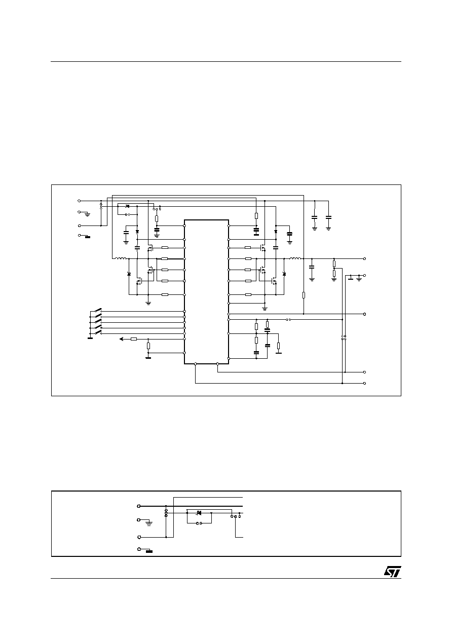
Demo Board Description
The L6919E demo board shows the operation of the device in a dual phase application. This evaluation board
allows output voltage adjustability (0.800V - 1.550V) through the switches S0-S4 and high output current capa-
bility.
The board has been laid out with the possibility to use up to two D2PACK mosfets for the low side switch in order
to give maximum flexibility in the mosfet choice.
The four layers demo board's copper thickness is of 70
m in order to minimize conduction losses considering
the high current that the circuit is able to deliver.
Demo board schematic circuit is reported in Figure 19.
Figure 19. Demo Board Schematic
Several jumpers allow setting different configurations for the device: JP3, JP4 and JP5 allow configuring the
remote buffer as desired. Simply shorting JP4 and JP5 the remote buffer is enabled and it senses the output
voltage on-board; to implement a real remote sense, leave these jumpers open and connect the FBG and FBR
connectors on the demo board to the remote load. To avoid using the remote buffer, simply short all the jumpers
JP3, JP4 and JP5. Local sense through the R7 is used for the regulation.
The input can be configured in different ways using the jumpers JP1, JP2 and JP6; these jumpers control also
the mosfet driver supply voltage. Anyway, power conversion starts from VIN and the device is supplied from VCC
(See Figure 20).
Figure 20. Power supply configuration
PGOOD
PGND
PGNDS2
ISEN2
LGATE2
VSEN
FB
PHASE2
UGATE2
BOOT2
VCC
COMP
SGND
OSC / INH
VID0
VID1
VID2
VID3
VID4
PGNDS1
ISEN1
LGATE1
PHASE1
UGATE1
BOOT1
VCCDR
6
24
25
26
27
16
15
2
5
4
3
1
13
14
22
21
20
18
19
7
28
23
10
9
8
11
12
FBR
FBG
17
C1
R7
R8
C2
R4
R3
Q3
Q4
C3
L2
C7
R11
D3
C6
C11..C13
C14,
C23
R1
JP3
R2
S1
S0
S3
S2
S4
R5
R6
Q1
L1
Q2
C4
D4
C5
Vin
GNDin
GNDCORE
VoutCORE
PGOOD
FBG
FBR
U1
L6919E
DZ1
C8
JP2
JP1
R13
R15
R12
R14
C9,C10
R9
R18
D1
R17
R16
Q1a
Q3a
D2
R19
R20
JP5
JP4
Vcc
GNDcc
JP6
To pin
VCC
R21
R10
C24
Vin
GNDin
DZ1
JP2
JP1
Vcc
GNDcc
JP6
To Vcc pin
To HS Drains (Power Input)
To BOOTx (HS Driver Supply)
To VCCDR pin (LS Driver Supply)
相关PDF资料 |
PDF描述 |
|---|---|
| LUW025F8 | 1-OUTPUT 16.5 W DC-DC REG PWR SUPPLY MODULE |
| L5973ADTR | 2.3 A SWITCHING REGULATOR, PDSO8 |
| LSN-1.8/10-D12BH | DC-DC REG PWR SUPPLY MODULE |
| LM2575-33IN | 4 A SWITCHING REGULATOR, 63 kHz SWITCHING FREQ-MAX, PDIP16 |
| LM2575IKTT | 4 A SWITCHING REGULATOR, 63 kHz SWITCHING FREQ-MAX, PSSO5 |
相关代理商/技术参数 |
参数描述 |
|---|---|
| L-692 | 制造商:RHOMBUS-IND 制造商全称:Rhombus Industries Inc. 功能描述:Common Mode Inductor |
| L6920 | 制造商:STMICROELECTRONICS 制造商全称:STMicroelectronics 功能描述:1V HIGH EFFICIENCY SYNCRONOUS STEP UP CONVERTER |
| L6920D | 功能描述:直流/直流开关转换器 0.6 to 5.5V Step-Up RoHS:否 制造商:STMicroelectronics 最大输入电压:4.5 V 开关频率:1.5 MHz 输出电压:4.6 V 输出电流:250 mA 输出端数量:2 最大工作温度:+ 85 C 安装风格:SMD/SMT |
| L6920DB | 功能描述:直流/直流开关转换器 Synchronous Rectifer Step Up Converter RoHS:否 制造商:STMicroelectronics 最大输入电压:4.5 V 开关频率:1.5 MHz 输出电压:4.6 V 输出电流:250 mA 输出端数量:2 最大工作温度:+ 85 C 安装风格:SMD/SMT |
| L6920DBTR | 功能描述:直流/直流开关转换器 SYNCRONOUS RECT. STEP UP CONVERTER RoHS:否 制造商:STMicroelectronics 最大输入电压:4.5 V 开关频率:1.5 MHz 输出电压:4.6 V 输出电流:250 mA 输出端数量:2 最大工作温度:+ 85 C 安装风格:SMD/SMT |
发布紧急采购,3分钟左右您将得到回复。