- 您现在的位置:买卖IC网 > PDF目录9165 > LMK04033BISQE/NOPB (National Semiconductor)IC CLOCK CONDITIONER PREC 48LLP PDF资料下载
参数资料
| 型号: | LMK04033BISQE/NOPB |
| 厂商: | National Semiconductor |
| 文件页数: | 30/65页 |
| 文件大小: | 0K |
| 描述: | IC CLOCK CONDITIONER PREC 48LLP |
| 标准包装: | 1 |
| 系列: | PowerWise® |
| 类型: | 时钟调节器 |
| PLL: | 是 |
| 输入: | LVCMOS |
| 输出: | LVCMOS,LVDS,2VPECL,LVPECL |
| 电路数: | 1 |
| 比率 - 输入:输出: | 2:6 |
| 差分 - 输入:输出: | 是/是 |
| 频率 - 最大: | 2.16GHz |
| 除法器/乘法器: | 是/是 |
| 电源电压: | 3.15 V ~ 3.45 V |
| 工作温度: | -40°C ~ 85°C |
| 安装类型: | 表面贴装 |
| 封装/外壳: | 48-WFQFN 裸露焊盘 |
| 供应商设备封装: | 48-LLP(7x7) |
| 包装: | 标准包装 |
| 产品目录页面: | 1275 (CN2011-ZH PDF) |
| 其它名称: | LMK04033BISQEDKR |
第1页第2页第3页第4页第5页第6页第7页第8页第9页第10页第11页第12页第13页第14页第15页第16页第17页第18页第19页第20页第21页第22页第23页第24页第25页第26页第27页第28页第29页当前第30页第31页第32页第33页第34页第35页第36页第37页第38页第39页第40页第41页第42页第43页第44页第45页第46页第47页第48页第49页第50页第51页第52页第53页第54页第55页第56页第57页第58页第59页第60页第61页第62页第63页第64页第65页
SNOSAZ8J – SEPTEMBER 2008 – REVISED SEPTEMBER 2011
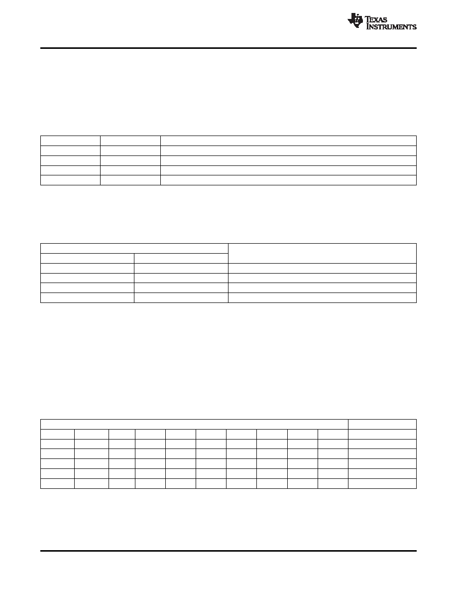
PLL1 Reference Clock LOS Timeout Control
This register is used to tune the LOS timeout based upon the frequency of the reference clock input(s). The
register value controls the timeout setting for both CLKin0 and CLKin1. The value programmed in the
LOS_TIMEOUT register represents the minimum input frequency for which loss of signal can be detected. For
example, if the reference input frequency is 12.288 MHz, then either register values (0,0) or (0,1) will result in
valid loss of signal detection. If the reference input frequency is 1 MHz, then only the register value (0,0) will
result in valid detection of signal loss.
Table 14. Reference Clock LOS Timeout Control Bits
b1
b0
Corresponding Minimum Input Frequency
0
1 MHz
0
1
3.0 MHz
1
0
13 MHz
1
32 MHz
LOS Output Type Control
The output format of the LOS pins may be selected as active CMOS, open drain NMOS and open drain PMOS,
as shown in the following table.
Table 15. Loss of Signal (LOS) Output Pin Format Type
LOS_TYPE [1:0]
Functional Description
b1
b0
0
Reserved
0
1
NMOS open drain
1
0
PMOS open drain
1
Active CMOS
The LOS output signal is valid only when CLKin_SEL bits are set to either [1,0] or [1,1]. If the CLKin_SEL field is
programmed to either of the fixed inputs, [0,0] or [0,1], the LOS_TYPE bits should be set to [0,0].
Register 12
PLL1_N: PLL1_N Counter
The size of the PLL1_N counter is 12 bits. This counter will support a maximum divide ratio of 4095 and
minimum divide ratio of 1. The 12 bit resolution is sufficient to support minimum phase detector frequency
resolution of approximately 50 kHz when the VCXO frequency is 200 MHz.
For a 200 MHz external VCXO, the minimum phase detector rate will be PDmin = 200 MHz/4095 = 48.84 kHz
Table 16. PLL1_N Counter Values
N [17:0]
VALUE
b11
b10
...
b6
b5
b4
b3
b2
b1
b0
0
Not Valid
0
1
0
1
0
2
.
...
1
4095
36
Copyright 2008–2011, Texas Instruments Incorporated
相关PDF资料 |
PDF描述 |
|---|---|
| MS27468E21A2P | CONN RCPT 65POS JAM NUT W/PINS |
| VI-BWL-MY-F4 | CONVERTER MOD DC/DC 28V 50W |
| VI-BWL-MY-F3 | CONVERTER MOD DC/DC 28V 50W |
| AD5204BR100 | IC DGTL POT QUAD 256POS 24-SOIC |
| AD5204BN50 | IC DGTL POT QUAD 256POS 24-DIP |
相关代理商/技术参数 |
参数描述 |
|---|---|
| LMK04033BISQX | 制造商:NSC 制造商全称:National Semiconductor 功能描述:Low-Noise Clock Jitter Cleaner with Cascaded PLLs |
| LMK04033BISQX/NOPB | 功能描述:时钟合成器/抖动清除器 RoHS:否 制造商:Skyworks Solutions, Inc. 输出端数量: 输出电平: 最大输出频率: 输入电平: 最大输入频率:6.1 GHz 电源电压-最大:3.3 V 电源电压-最小:2.7 V 封装 / 箱体:TSSOP-28 封装:Reel |
| LMK04100 | 制造商:TI 制造商全称:Texas Instruments 功能描述:LMK04100 Family Clock Jitter Cleaner with Cascaded PLLs |
| LMK04100EVAL/NOPB | 功能描述:时钟和定时器开发工具 LMK04100 Eval Mod RoHS:否 制造商:Texas Instruments 产品:Evaluation Modules 类型:Clock Conditioners 工具用于评估:LMK04100B 频率:122.8 MHz 工作电源电压:3.3 V |
| LMK04100SQ/NOPB | 功能描述:时钟合成器/抖动清除器 RoHS:否 制造商:Skyworks Solutions, Inc. 输出端数量: 输出电平: 最大输出频率: 输入电平: 最大输入频率:6.1 GHz 电源电压-最大:3.3 V 电源电压-最小:2.7 V 封装 / 箱体:TSSOP-28 封装:Reel |
发布紧急采购,3分钟左右您将得到回复。