- 您现在的位置:买卖IC网 > PDF目录9165 > LMK04033BISQE/NOPB (National Semiconductor)IC CLOCK CONDITIONER PREC 48LLP PDF资料下载
参数资料
| 型号: | LMK04033BISQE/NOPB |
| 厂商: | National Semiconductor |
| 文件页数: | 41/65页 |
| 文件大小: | 0K |
| 描述: | IC CLOCK CONDITIONER PREC 48LLP |
| 标准包装: | 1 |
| 系列: | PowerWise® |
| 类型: | 时钟调节器 |
| PLL: | 是 |
| 输入: | LVCMOS |
| 输出: | LVCMOS,LVDS,2VPECL,LVPECL |
| 电路数: | 1 |
| 比率 - 输入:输出: | 2:6 |
| 差分 - 输入:输出: | 是/是 |
| 频率 - 最大: | 2.16GHz |
| 除法器/乘法器: | 是/是 |
| 电源电压: | 3.15 V ~ 3.45 V |
| 工作温度: | -40°C ~ 85°C |
| 安装类型: | 表面贴装 |
| 封装/外壳: | 48-WFQFN 裸露焊盘 |
| 供应商设备封装: | 48-LLP(7x7) |
| 包装: | 标准包装 |
| 产品目录页面: | 1275 (CN2011-ZH PDF) |
| 其它名称: | LMK04033BISQEDKR |
第1页第2页第3页第4页第5页第6页第7页第8页第9页第10页第11页第12页第13页第14页第15页第16页第17页第18页第19页第20页第21页第22页第23页第24页第25页第26页第27页第28页第29页第30页第31页第32页第33页第34页第35页第36页第37页第38页第39页第40页当前第41页第42页第43页第44页第45页第46页第47页第48页第49页第50页第51页第52页第53页第54页第55页第56页第57页第58页第59页第60页第61页第62页第63页第64页第65页
SNOSAZ8J – SEPTEMBER 2008 – REVISED SEPTEMBER 2011
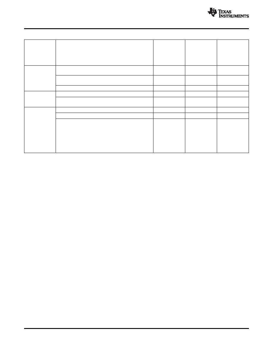
Table 33. Typical Current Consumption for Selected Functional Blocks (continued)
Power
Typical ICC
Power
Dissipated in
(Temp = 25 °C,
Dissipated in
LVPECL/2VPECL
Block
Condition
VCC = 3.3 V)
device
Emitter
(mA)
(mW)
Resistors
(mW)
LVPECL/2VPECL buffer (enabled and with 120
Ω emitter
40
82
50
resistors)
LVPECL/2VPECL
LVPECL/2VPECL buffer (disabled and with 120
Ω emitter
Buffer
21.7
47
25
resistors)
LVPECL/2VPECL (disabled and with no emitter resistors)
0
-
LVCMOS buffer static ICC, CL = 5 pF
4.5
15
-
LVCMOS Buffer
LVCMOS buffer dynamic ICC, CL = 5 pF, CLKout = 100
(1)
16
53
-
MHz
Entire device
LMK0400x (2) (3)
379.5
1102
150
(Single input clock
LMK0401x (2) (3)
377.5
996
250
(CLKIN_SEL = 0
LMK0403x (2) (3)
or 1); LOS
disabled; PLL1
and PLL2 locked;
Fout disabled; All
337.1
1012
100
CLKouts are on;
No delay); Divide
> 2 on each
output.
(1)
Dynamic power dissipation of LVCMOS buffer varies with output frequency and can be found in the LVCMOS dynamic ICC vs frequency
plot, as shown in Typical Performance Characteristics. Total power dissipation of the LVCMOS buffer is the sum of static and dynamic
power dissipation. CLKoutXa and CLKoutXb are each considered an LVCMOS buffer.
(2)
Assuming ThetaJ = 27.4 °C/W, the total power dissipated on chip must be less than 40/27.4 = 1450 mW to guarantee a junction
temperature is less than 125 °C.
(3)
Worst case power dissipation can be estimated by multiplying typical power dissipation with a factor of 1.2.
Current Consumption / Power Dissipation Calculations
Due to the myriad of possible configurations the following table serves to provide enough information to allow the
user to calculate estimated current consumption of the device. Unless otherwise noted VCC = 3.3 V, TA = 25 °C.
From Table 33 the current consumption can be calculated in any configuration. For example, the current for the
entire device with 1 LVDS (CLKout0) & 1 LVPECL (CLKout1) output in bypassed mode can be calculated by
adding up the following blocks: core current, clock buffer, one LVDS output buffer current, and one LVPECL
output buffer current. There will also be one LVPECL output drawing emitter current, but some of the power from
the current draw is dissipated in the external 120
Ω resistors which doesn't add to the power dissipation budget
for the device. If delays or divides are switched in, then the additional current for these stages needs to be added
as well.
For power dissipated by the device, the total current entering the device is multiplied by the voltage at the device
minus the power dissipated in any emitter resistors connected to any of the LVPECL outputs. If no emitter
resistors are connected to the LVPECL outputs, this power will be 0 watts. For example, in the case of 1 LVDS
(CLKout0) & 1 LVPECL (CLKout1) operating at 3.3 V, we calculate 3.3 V × (115 + 10 + 10 + 19.3 + 40) mA = 3.3
V × 194.3 mA = 641.2 mW. Because the LVPECL output (CLKout1) has the emitter resistors hooked up and the
power dissipated by these resistors is 50 mW, the total device power dissipation is 641.2 mW - 50 mW = 591.2
mW.
When the LVPECL output is active, ~1.7 V is the average voltage on each output as calculated from the LVPECL
VOH & VOL typical specification. Therefore the power dissipated in each emitter resistor is approximately (1.7 V)
2 /
120
Ω = 25 mW. When the LVPECL output is disabled, the emitter resistor voltage is ~1.07 V. Therefore the
power dissipated in each emitter resistor is approximately (1.07 V)2 / 120
Ω = 9.5 mW.
46
Copyright 2008–2011, Texas Instruments Incorporated
相关PDF资料 |
PDF描述 |
|---|---|
| MS27468E21A2P | CONN RCPT 65POS JAM NUT W/PINS |
| VI-BWL-MY-F4 | CONVERTER MOD DC/DC 28V 50W |
| VI-BWL-MY-F3 | CONVERTER MOD DC/DC 28V 50W |
| AD5204BR100 | IC DGTL POT QUAD 256POS 24-SOIC |
| AD5204BN50 | IC DGTL POT QUAD 256POS 24-DIP |
相关代理商/技术参数 |
参数描述 |
|---|---|
| LMK04033BISQX | 制造商:NSC 制造商全称:National Semiconductor 功能描述:Low-Noise Clock Jitter Cleaner with Cascaded PLLs |
| LMK04033BISQX/NOPB | 功能描述:时钟合成器/抖动清除器 RoHS:否 制造商:Skyworks Solutions, Inc. 输出端数量: 输出电平: 最大输出频率: 输入电平: 最大输入频率:6.1 GHz 电源电压-最大:3.3 V 电源电压-最小:2.7 V 封装 / 箱体:TSSOP-28 封装:Reel |
| LMK04100 | 制造商:TI 制造商全称:Texas Instruments 功能描述:LMK04100 Family Clock Jitter Cleaner with Cascaded PLLs |
| LMK04100EVAL/NOPB | 功能描述:时钟和定时器开发工具 LMK04100 Eval Mod RoHS:否 制造商:Texas Instruments 产品:Evaluation Modules 类型:Clock Conditioners 工具用于评估:LMK04100B 频率:122.8 MHz 工作电源电压:3.3 V |
| LMK04100SQ/NOPB | 功能描述:时钟合成器/抖动清除器 RoHS:否 制造商:Skyworks Solutions, Inc. 输出端数量: 输出电平: 最大输出频率: 输入电平: 最大输入频率:6.1 GHz 电源电压-最大:3.3 V 电源电压-最小:2.7 V 封装 / 箱体:TSSOP-28 封装:Reel |
发布紧急采购,3分钟左右您将得到回复。