- 您现在的位置:买卖IC网 > PDF目录9165 > LMK04033BISQE/NOPB (National Semiconductor)IC CLOCK CONDITIONER PREC 48LLP PDF资料下载
参数资料
| 型号: | LMK04033BISQE/NOPB |
| 厂商: | National Semiconductor |
| 文件页数: | 48/65页 |
| 文件大小: | 0K |
| 描述: | IC CLOCK CONDITIONER PREC 48LLP |
| 标准包装: | 1 |
| 系列: | PowerWise® |
| 类型: | 时钟调节器 |
| PLL: | 是 |
| 输入: | LVCMOS |
| 输出: | LVCMOS,LVDS,2VPECL,LVPECL |
| 电路数: | 1 |
| 比率 - 输入:输出: | 2:6 |
| 差分 - 输入:输出: | 是/是 |
| 频率 - 最大: | 2.16GHz |
| 除法器/乘法器: | 是/是 |
| 电源电压: | 3.15 V ~ 3.45 V |
| 工作温度: | -40°C ~ 85°C |
| 安装类型: | 表面贴装 |
| 封装/外壳: | 48-WFQFN 裸露焊盘 |
| 供应商设备封装: | 48-LLP(7x7) |
| 包装: | 标准包装 |
| 产品目录页面: | 1275 (CN2011-ZH PDF) |
| 其它名称: | LMK04033BISQEDKR |
第1页第2页第3页第4页第5页第6页第7页第8页第9页第10页第11页第12页第13页第14页第15页第16页第17页第18页第19页第20页第21页第22页第23页第24页第25页第26页第27页第28页第29页第30页第31页第32页第33页第34页第35页第36页第37页第38页第39页第40页第41页第42页第43页第44页第45页第46页第47页当前第48页第49页第50页第51页第52页第53页第54页第55页第56页第57页第58页第59页第60页第61页第62页第63页第64页第65页
CLKoutX
CLKoutX*
LVPECL
Receiver
1
2
0:
100: Trace
(Differential)
1
2
0:
Vcc
LVPECL
Driver
8
2:
8
2:
CLKoutX
CLKoutX*
LVPECL
Receiver
5
0:
100: Trace
(Differential)
5
0:
Vcc - 2 V
LVPECL
Driver
CLKoutX
CLKoutX*
LVDS
Receiver
1
0
0:
100: Trace
(Differential)
LVDS
Driver
SNOSAZ8J – SEPTEMBER 2008 – REVISED SEPTEMBER 2011
It is possible to drive a non-LVPECL or non-LVDS receiver with an LVDS or LVPECL driver as long as the above
guidelines are followed. Check the datasheet of the receiver or input being driven to determine the best
termination and coupling method to be sure that the receiver is biased at its optimum DC voltage (common mode
voltage). For example, when driving the OSCin/OSCin* input of the LMK04000 family, OSCin/OSCin* should be
AC coupled because OSCin/OSCin* biases the signal to the proper DC level (See Figure 13) This is only slightly
different from the AC coupled cases described in Driving CLKin Pins with a Single-Ended Source because the
DC blocking capacitors are placed between the termination and the OSCin/OSCin* pins, but the concept remains
the same. The receiver (OSCin/OSCin*) sets the input to the optimum DC bias voltage (common mode voltage),
not the driver.
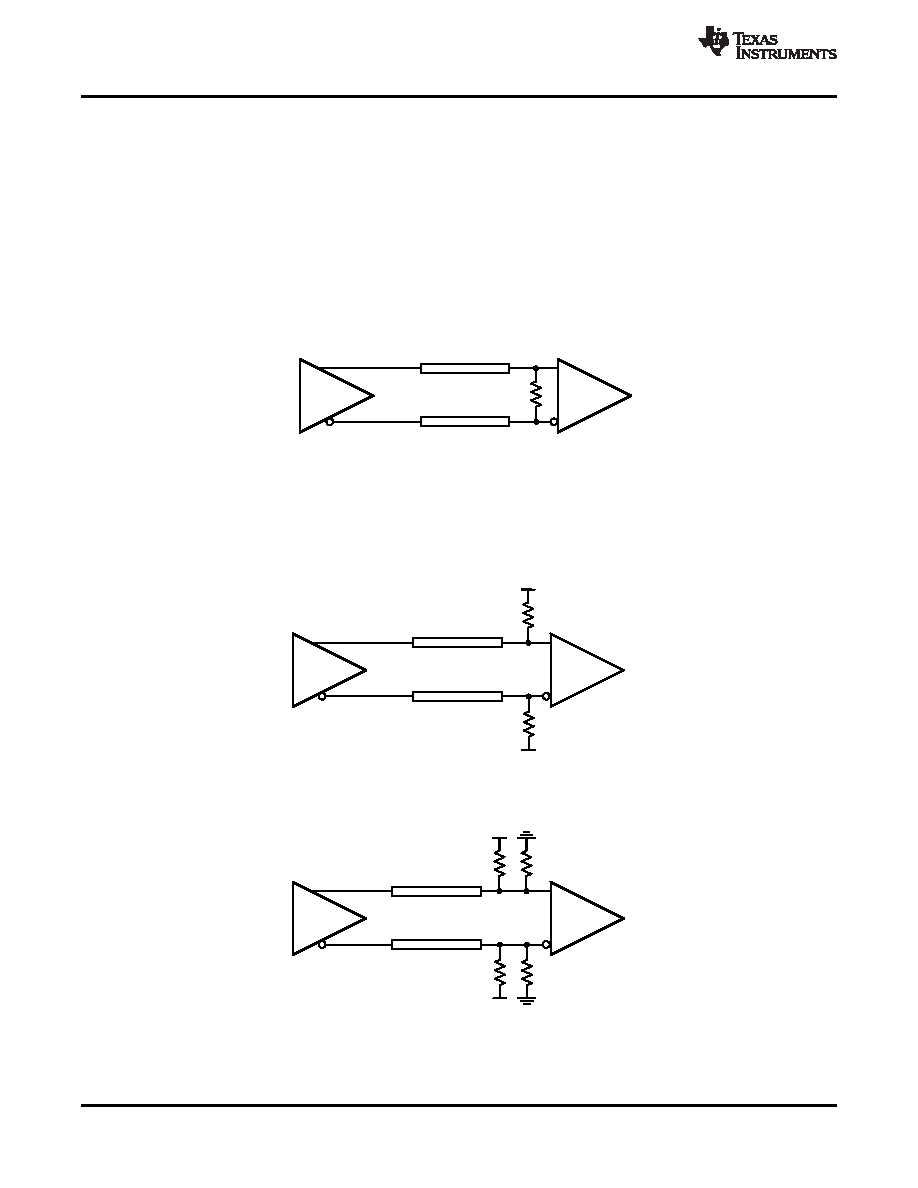
Termination for DC Coupled Differential Operation
For DC coupled operation of an LVDS driver, terminate with 100
Ω as close as possible to the LVDS receiver as
shown in Figure 18.
Figure 18. Differential LVDS Operation, DC Coupling, No Biasing of the Receiver
For DC coupled operation of an LVPECL driver, terminate with 50
Alternatively terminate with a Thevenin equivalent circuit (120
Ω resistor connected to VCC and an 82 Ω resistor
connected to ground with the driver connected to the junction of the 120
Ω and 82 Ω resistors) as shown in
Figure 19. Differential LVPECL Operation, DC Coupling
Figure 20. Differential LVPECL Operation, DC Coupling, Thevenin Equivalent
52
Copyright 2008–2011, Texas Instruments Incorporated
相关PDF资料 |
PDF描述 |
|---|---|
| MS27468E21A2P | CONN RCPT 65POS JAM NUT W/PINS |
| VI-BWL-MY-F4 | CONVERTER MOD DC/DC 28V 50W |
| VI-BWL-MY-F3 | CONVERTER MOD DC/DC 28V 50W |
| AD5204BR100 | IC DGTL POT QUAD 256POS 24-SOIC |
| AD5204BN50 | IC DGTL POT QUAD 256POS 24-DIP |
相关代理商/技术参数 |
参数描述 |
|---|---|
| LMK04033BISQX | 制造商:NSC 制造商全称:National Semiconductor 功能描述:Low-Noise Clock Jitter Cleaner with Cascaded PLLs |
| LMK04033BISQX/NOPB | 功能描述:时钟合成器/抖动清除器 RoHS:否 制造商:Skyworks Solutions, Inc. 输出端数量: 输出电平: 最大输出频率: 输入电平: 最大输入频率:6.1 GHz 电源电压-最大:3.3 V 电源电压-最小:2.7 V 封装 / 箱体:TSSOP-28 封装:Reel |
| LMK04100 | 制造商:TI 制造商全称:Texas Instruments 功能描述:LMK04100 Family Clock Jitter Cleaner with Cascaded PLLs |
| LMK04100EVAL/NOPB | 功能描述:时钟和定时器开发工具 LMK04100 Eval Mod RoHS:否 制造商:Texas Instruments 产品:Evaluation Modules 类型:Clock Conditioners 工具用于评估:LMK04100B 频率:122.8 MHz 工作电源电压:3.3 V |
| LMK04100SQ/NOPB | 功能描述:时钟合成器/抖动清除器 RoHS:否 制造商:Skyworks Solutions, Inc. 输出端数量: 输出电平: 最大输出频率: 输入电平: 最大输入频率:6.1 GHz 电源电压-最大:3.3 V 电源电压-最小:2.7 V 封装 / 箱体:TSSOP-28 封装:Reel |
发布紧急采购,3分钟左右您将得到回复。