参数资料
| 型号: | LT1977IFE#TRPBF |
| 厂商: | Linear Technology |
| 文件页数: | 17/24页 |
| 文件大小: | 0K |
| 描述: | IC REG BUCK ADJ 1.5A 16TSSOP |
| 标准包装: | 2,500 |
| 类型: | 降压(降压) |
| 输出类型: | 可调式 |
| 输出数: | 1 |
| 输出电压: | 1.2 V ~ 54 V |
| 输入电压: | 3.3 V ~ 60 V |
| PWM 型: | 电流模式,混合 |
| 频率 - 开关: | 500kHz |
| 电流 - 输出: | 1.5A |
| 同步整流器: | 无 |
| 工作温度: | -40°C ~ 125°C |
| 安装类型: | 表面贴装 |
| 封装/外壳: | 16-TSSOP(0.173",4.40mm)裸露焊盘 |
| 包装: | 带卷 (TR) |
| 供应商设备封装: | 16-TSSOP-EP |
�� �
�
�LT1977�
�APPLICATIO� S� I� FOR� ATIO�
�must� weigh� the� importance� of� each� specification� in� choos-�
�ing� the� best� diode� for� the� application.�
�OPTIONAL�
�The� use� of� so-called� “ultrafast”� recovery� diodes� is� gener-�
�ally� not� recommended.� When� operating� in� continuous�
�mode,� the� reverse� recovery� time� exhibited� by� “ultrafast”�
�V� IN�
�V� IN� BOOST�
�LT1977�
�GND�
�SW�
�V� OUT�
�diodes� will� result� in� a� slingshot� type� effect.� The� power�
�internal� switch� will� ramp� up� V� IN� current� into� the� diode� in� an�
�attempt� to� get� it� to� recover.� Then,� when� the� diode� has�
�finally� turned� off,� some� tens� of� nanoseconds� later,� the� V� SW�
�node� voltage� ramps� up� at� an� extremely� high� dV/dt,� per-�
�V� BOOST� –� V� SW� =� V� OUT�
�V� BOOST(MAX)� =� V� IN� +� V� OUT�
�(7a)�
�haps� 5V� to� even� 10V/ns!� With� real� world� lead� inductances�
�the� V� SW� node� can� easily� overshoot� the� V� IN� rail.� This� can�
�V� IN�
�V� IN� BOOST�
�LT1977�
�result� in� poor� RFI� behavior� and,� if� the� overshoot� is� severe�
�GND�
�SW�
�V� OUT�
�enough,� damage� the� IC� itself.�
�V� BOOST� –� V� SW� =� V� IN�
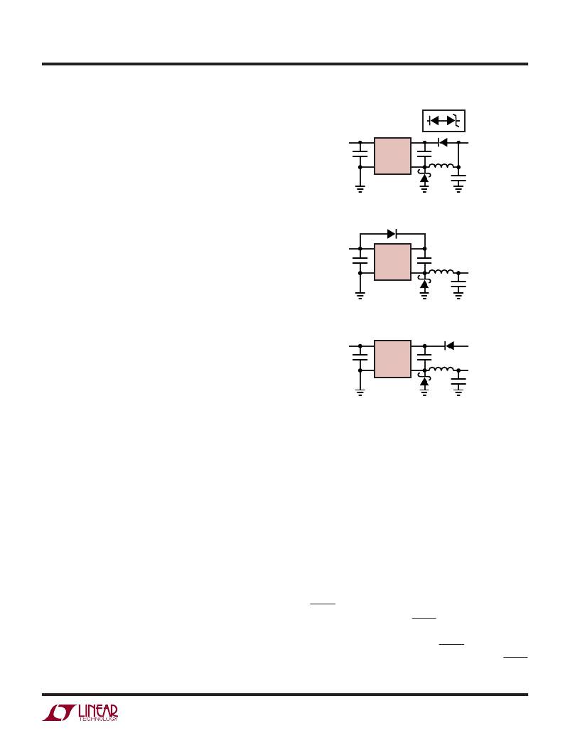
�BOOST� PIN�
�For� most� applications� the� boost� components� are� a� 0.1� μ� F�
�V� BOOST(MAX)� =� 2V� IN�
�(7b)�
�capacitor� and� a� MMSD914� diode.� The� anode� is� typically�
�connected� to� the� regulated� output� voltage� to� generate� a�
�V� IN�
�V� IN� BOOST�
�LT1977�
�V� DC�
�voltage� approximately� V� OUT� above� V� IN� to� drive� the� output�
�stage� (Figure� 7a).� However,� the� output� stage� discharges�
�GND�
�SW�
�D� SS�
�V� OUT�
�the� boost� capacitor� during� the� on� time� of� the� switch.� The�
�V� BOOST� –� V� SW� =� V� DC�
�1977� F07�
�output� driver� requires� at� least� 2.5V� of� headroom� through-�
�out� this� period� to� keep� the� switch� fully� saturated.� If� the�
�output� voltage� is� less� than� 3.3V� it� is� recommended� that� an�
�alternate� boost� supply� is� used.� The� boost� diode� can� be�
�connected� to� the� input� (Figure� 7b)� but� care� must� be� taken�
�to� prevent� the� boost� voltage� (V� BOOST� =� V� IN� ?� 2)� from�
�exceeding� the� BOOST� pin� absolute� maximum� rating.� The�
�additional� voltage� across� the� switch� driver� also� increases�
�power� loss� and� reduces� efficiency.� If� available,� an� inde-�
�pendent� supply� can� be� used� to� generate� the� required�
�BOOST� voltage� (Figure� 7c).� Tying� BOOST� to� V� IN� or� an�
�independent� supply� may� reduce� efficiency� but� it� will� re-�
�duce� the� minimum� V� IN� required� to� start-up� with� light�
�loads.� If� the� generated� BOOST� voltage� dissipates� too�
�much� power� at� maximum� load,� the� BOOST� voltage� the�
�LT1977� sees� can� be� reduced� by� placing� a� Zener� diode� in�
�series� with� the� BOOST� diode� (Figure� 7a� option).�
�A� 0.1� μ� F� boost� capacitor� is� recommended� for� most� appli-�
�cations.� Almost� any� type� of� film� or� ceramic� capacitor� is�
�suitable� but� the� ESR� should� be� <1� ?� to� ensure� it� can� be� fully�
�recharged� during� the� off� time� of� the� switch.� The� capacitor�
�V� BOOST(MAX)� =� V� DC� +� V� IN�
�(7c)�
�Figure� 7.� BOOST� Pin� Configurations�
�value� is� derived� from� worst-case� conditions� of� 1800ns� on�
�time,� 40mA� boost� current� and� 0.7V� discharge� ripple.� The�
�boost� capacitor� value� could� be� reduced� under� less� de-�
�manding� conditions� but� this� will� not� improve� circuit� opera-�
�tion� or� efficiency.� Under� low� input� voltage� and� low� load�
�conditions� a� higher� value� capacitor� will� reduce� discharge�
�ripple� and� improve� start-up� operation.�
�SHUTDOWN� FUNCTION� AND� UNDERVOLTAGE�
�LOCKOUT�
�The� SHDN� pin� on� the� LT1977� controls� the� operation� of� the�
�IC.� When� the� voltage� on� the� SHDN� pin� is� below� the� 1.2V�
�shutdown� threshold� the� LT1977� is� placed� in� a� “zero”�
�supply� current� state.� Driving� the� SHDN� pin� above� the�
�shutdown� threshold� enables� normal� operation.� The� SHDN�
�pin� has� an� internal� sink� current� of� 3� μ� A.�
�1977fa�
�17�
�相关PDF资料 |
PDF描述 |
|---|---|
| LT3008EDC-1.2#TRMPBF | IC REG LDO 1.2V 20MA 6-DFN |
| LT3009ESC8-1.5#TRMPBF | IC REG LDO 1.5V 20MA SC70-8 |
| LT3010MPMS8E-5#TRPBF | IC REG LDO 5V 50MA 8-MSOP |
| LT3011HMSE#TRPBF | IC REG LDO ADJ 50MA 12-MSOP |
| LT3012HFE#TRPBF | IC REG LDO ADJ .2A 16-TSSOP |
相关代理商/技术参数 |
参数描述 |
|---|---|
| LT1990 | 制造商:LINER 制造商全称:Linear Technology 功能描述:Precision, 100μA Gain Selectable Amplifier |
| LT1990ACS8 | 功能描述:IC AMP DIFF +/-250V MCRPWR 8SOIC RoHS:否 类别:集成电路 (IC) >> Linear - Amplifiers - Instrumentation 系列:- 标准包装:1 系列:- 放大器类型:通用 电路数:4 输出类型:满摆幅 转换速率:0.6 V/µs 增益带宽积:1MHz -3db带宽:- 电流 - 输入偏压:2pA 电压 - 输入偏移:1000µV 电流 - 电源:85µA 电流 - 输出 / 通道:20mA 电压 - 电源,单路/双路(±):1.8 V ~ 6 V 工作温度:-40°C ~ 125°C 安装类型:表面贴装 封装/外壳:14-SOIC(0.154",3.90mm 宽) 供应商设备封装:14-SOICN 包装:剪切带 (CT) 产品目录页面:680 (CN2011-ZH PDF) 其它名称:MCP6L04T-E/SLCT |
| LT1990ACS8#PBF | 功能描述:IC AMP DIFF +/-250V MCRPWR 8SOIC RoHS:是 类别:集成电路 (IC) >> Linear - Amplifiers - Instrumentation 系列:- 产品培训模块:Differential Circuit Design Techniques for Communication Applications 标准包装:1 系列:- 放大器类型:RF/IF 差分 电路数:1 输出类型:差分 转换速率:9800 V/µs 增益带宽积:- -3db带宽:2.9GHz 电流 - 输入偏压:3µA 电压 - 输入偏移:- 电流 - 电源:40mA 电流 - 输出 / 通道:- 电压 - 电源,单路/双路(±):3 V ~ 3.6 V 工作温度:-40°C ~ 85°C 安装类型:表面贴装 封装/外壳:16-VQFN 裸露焊盘,CSP 供应商设备封装:16-LFCSP-VQ 包装:剪切带 (CT) 产品目录页面:551 (CN2011-ZH PDF) 其它名称:ADL5561ACPZ-R7CT |
| LT1990ACS8#TR | 功能描述:IC AMP DIFF +/-250V MCRPWR 8SOIC RoHS:否 类别:集成电路 (IC) >> Linear - Amplifiers - Instrumentation 系列:- 标准包装:1 系列:- 放大器类型:通用 电路数:4 输出类型:满摆幅 转换速率:0.6 V/µs 增益带宽积:1MHz -3db带宽:- 电流 - 输入偏压:2pA 电压 - 输入偏移:1000µV 电流 - 电源:85µA 电流 - 输出 / 通道:20mA 电压 - 电源,单路/双路(±):1.8 V ~ 6 V 工作温度:-40°C ~ 125°C 安装类型:表面贴装 封装/外壳:14-SOIC(0.154",3.90mm 宽) 供应商设备封装:14-SOICN 包装:剪切带 (CT) 产品目录页面:680 (CN2011-ZH PDF) 其它名称:MCP6L04T-E/SLCT |
| LT1990ACS8#TRPBF | 功能描述:IC AMP DIFF +/-250V MCRPWR 8SOIC RoHS:是 类别:集成电路 (IC) >> Linear - Amplifiers - Instrumentation 系列:- 标准包装:1 系列:- 放大器类型:通用 电路数:4 输出类型:满摆幅 转换速率:0.6 V/µs 增益带宽积:1MHz -3db带宽:- 电流 - 输入偏压:2pA 电压 - 输入偏移:1000µV 电流 - 电源:85µA 电流 - 输出 / 通道:20mA 电压 - 电源,单路/双路(±):1.8 V ~ 6 V 工作温度:-40°C ~ 125°C 安装类型:表面贴装 封装/外壳:14-SOIC(0.154",3.90mm 宽) 供应商设备封装:14-SOICN 包装:剪切带 (CT) 产品目录页面:680 (CN2011-ZH PDF) 其它名称:MCP6L04T-E/SLCT |
发布紧急采购,3分钟左右您将得到回复。