参数资料
| 型号: | LT1977IFE#TRPBF |
| 厂商: | Linear Technology |
| 文件页数: | 3/24页 |
| 文件大小: | 0K |
| 描述: | IC REG BUCK ADJ 1.5A 16TSSOP |
| 标准包装: | 2,500 |
| 类型: | 降压(降压) |
| 输出类型: | 可调式 |
| 输出数: | 1 |
| 输出电压: | 1.2 V ~ 54 V |
| 输入电压: | 3.3 V ~ 60 V |
| PWM 型: | 电流模式,混合 |
| 频率 - 开关: | 500kHz |
| 电流 - 输出: | 1.5A |
| 同步整流器: | 无 |
| 工作温度: | -40°C ~ 125°C |
| 安装类型: | 表面贴装 |
| 封装/外壳: | 16-TSSOP(0.173",4.40mm)裸露焊盘 |
| 包装: | 带卷 (TR) |
| 供应商设备封装: | 16-TSSOP-EP |
�� �
�
�LT1977�
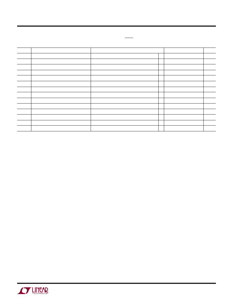
�ELECTRICAL� CHARACTERISTICS� The� ●� denotes� the� specifications� which� apply� over� the� full� operating�
�temperature� range,� otherwise� specifications� are� at� T� J� =� 25� °� C.� V� IN� =� 12V,� SHDN� =� 12V,� BIAS� =� 5V,� FB/PGFB� =� 1.25V,� C� SS� /SYNC� =� 0V�
�unless� otherwise� noted.�
�SYMBOL�
�PARAMETER�
�Switch� On� Resistance� (Note� 9)�
�Switching� Frequency�
�CONDITIONS�
�●�
�●�
�MIN�
�425�
�TYP�
�0.2�
�500�
�MAX�
�0.4�
�575�
�UNITS�
�?�
�kHz�
�Maximum� Duty� Cycle�
�86�
�92�
�%�
�Minimum� SYNC� Amplitude�
�SYNC� Frequency� Range�
�SYNC� Input� Impedance�
�575�
�1.5�
�85�
�2.0�
�700�
�V�
�kHz�
�k� ?�
�I� CSS�
�I� PGFB�
�V� PGFB�
�I� CT�
�C� SS� Current� Threshold� (Note� 10)�
�PGFB� Input� Current�
�PGFB� Voltage� Threshold� (Note� 11)�
�C� T� Source� Current� (Note� 11)�
�FB� =� 0V�
�●�
�7�
�88�
�2�
�13�
�25�
�90�
�3.6�
�20�
�100�
�92�
�5.5�
�μ� A�
�nA�
�%�
�μ� A�
�C� T� Sink� Current� (Note� 11)�
�1�
�2�
�mA�
�V� CT�
�C� T� Voltage� Threshold� (Note� 11)�
�PG� Leakage� (Note� 11)�
�PG� Sink� Current� (Note� 11)�
�V� PG� =� 12V�
�PGFB� =� 1V,� PG� =� 400mV�
�1.16�
�100�
�1.2�
�0.1�
�200�
�1.26�
�1�
�V�
�μ� A�
�μ� A�
�Note� 1:� Absolute� Maximum� Ratings� are� those� values� beyond� which� the� life�
�of� a� device� may� be� impaired.�
�Note� 2:� The� LT1977EFE� is� guaranteed� to� meet� performance� specifications�
�from� 0� °� C� to� 125� °� C� junction� temperature.� Specifications� over� the� –40� °� C� to�
�125� °� C� operating� junction� temperature� range� are� assured� by� design,�
�characterization� and� correlation� with� statistical� process� controls.� The�
�LT1977IFE� is� guaranteed� and� tested� over� the� full� –40� °� C� to� 125� °� C�
�operating� junction� temperature� range.�
�Note� 3:� Minimum� input� voltage� is� defined� as� the� voltage� where� switching�
�starts.� Actual� minimum� input� voltage� to� maintain� a� regulated� output� will�
�depend� upon� output� voltage� and� load� current.� See� Applications�
�Information.�
�Note� 4:� Supply� input� current� is� the� quiescent� current� drawn� by� the� input�
�pin.� Its� typical� value� depends� on� the� voltage� on� the� BIAS� pin� and� operating�
�state� of� the� LT1977.� With� the� BIAS� pin� at� 0V,� all� of� the� quiescent� current�
�required� to� operate� the� LT1977� will� be� provided� by� the� V� IN� pin.� With� the�
�BIAS� voltage� above� its� minimum� input� voltage,� a� portion� of� the� total�
�quiescent� current� will� be� supplied� by� the� BIAS� pin.� Supply� sleep� current� is�
�defined� as� the� quiescent� current� during� the� “sleep”� portion� of� Burst� Mode�
�operation.� See� Applications� Information� for� determining� application� supply�
�currents.�
�Note� 5:� Minimum� BIAS� voltage� is� the� voltage� on� the� BIAS� pin� when� I� BIAS� is�
�sourced� into� the� pin.�
�Note� 6:� This� is� the� minimum� voltage� across� the� boost� capacitor� needed� to�
�guarantee� full� saturation� of� the� internal� power� switch.�
�Note� 7:� Boost� current� is� the� current� flowing� into� the� BOOST� pin� with� the� pin�
�held� 3.3V� above� input� voltage.� It� flows� only� during� switch� on� time.�
�Note� 8:� Gain� is� measured� with� a� V� C� swing� from� 1.15V� to� 750mV.�
�Note� 9:� Switch� on� resistance� is� calculated� by� dividing� V� IN� to� SW� voltage� by� the�
�forced� current� (1.5A).� See� Typical� Performance� Characteristics� for� the� graph�
�of� switch� voltage� at� other� currents.�
�Note� 10:� The� C� SS� threshold� is� defined� as� the� value� of� current� sourced� into� the�
�C� SS� pin� which� results� in� an� increase� in� sink� current� from� the� V� C� pin.� See� the�
�Soft-Start� section� in� Applications� Information.�
�Note� 11:� The� PGFB� threshold� is� defined� as� the� percentage� of� V� REF� voltage�
�which� causes� the� current� source� output� of� the� C� T� pin� to� change� from�
�sinking� (below� threshold)� to� sourcing� current� (above� threshold).� When�
�sourcing� current,� the� voltage� on� the� C� T� pin� rises� until� it� is� clamped�
�internally.� When� the� clamp� is� activated,� the� output� of� the� PG� pin� will� be� set�
�to� a� high� impedance� state.� When� the� C� T� clamp� is� inactive� the� PG� pin� will�
�be� set� active� low� with� a� current� sink� capability� of� 200� μ� A.�
�1977fa�
�3�
�相关PDF资料 |
PDF描述 |
|---|---|
| LT3008EDC-1.2#TRMPBF | IC REG LDO 1.2V 20MA 6-DFN |
| LT3009ESC8-1.5#TRMPBF | IC REG LDO 1.5V 20MA SC70-8 |
| LT3010MPMS8E-5#TRPBF | IC REG LDO 5V 50MA 8-MSOP |
| LT3011HMSE#TRPBF | IC REG LDO ADJ 50MA 12-MSOP |
| LT3012HFE#TRPBF | IC REG LDO ADJ .2A 16-TSSOP |
相关代理商/技术参数 |
参数描述 |
|---|---|
| LT1990 | 制造商:LINER 制造商全称:Linear Technology 功能描述:Precision, 100μA Gain Selectable Amplifier |
| LT1990ACS8 | 功能描述:IC AMP DIFF +/-250V MCRPWR 8SOIC RoHS:否 类别:集成电路 (IC) >> Linear - Amplifiers - Instrumentation 系列:- 标准包装:1 系列:- 放大器类型:通用 电路数:4 输出类型:满摆幅 转换速率:0.6 V/µs 增益带宽积:1MHz -3db带宽:- 电流 - 输入偏压:2pA 电压 - 输入偏移:1000µV 电流 - 电源:85µA 电流 - 输出 / 通道:20mA 电压 - 电源,单路/双路(±):1.8 V ~ 6 V 工作温度:-40°C ~ 125°C 安装类型:表面贴装 封装/外壳:14-SOIC(0.154",3.90mm 宽) 供应商设备封装:14-SOICN 包装:剪切带 (CT) 产品目录页面:680 (CN2011-ZH PDF) 其它名称:MCP6L04T-E/SLCT |
| LT1990ACS8#PBF | 功能描述:IC AMP DIFF +/-250V MCRPWR 8SOIC RoHS:是 类别:集成电路 (IC) >> Linear - Amplifiers - Instrumentation 系列:- 产品培训模块:Differential Circuit Design Techniques for Communication Applications 标准包装:1 系列:- 放大器类型:RF/IF 差分 电路数:1 输出类型:差分 转换速率:9800 V/µs 增益带宽积:- -3db带宽:2.9GHz 电流 - 输入偏压:3µA 电压 - 输入偏移:- 电流 - 电源:40mA 电流 - 输出 / 通道:- 电压 - 电源,单路/双路(±):3 V ~ 3.6 V 工作温度:-40°C ~ 85°C 安装类型:表面贴装 封装/外壳:16-VQFN 裸露焊盘,CSP 供应商设备封装:16-LFCSP-VQ 包装:剪切带 (CT) 产品目录页面:551 (CN2011-ZH PDF) 其它名称:ADL5561ACPZ-R7CT |
| LT1990ACS8#TR | 功能描述:IC AMP DIFF +/-250V MCRPWR 8SOIC RoHS:否 类别:集成电路 (IC) >> Linear - Amplifiers - Instrumentation 系列:- 标准包装:1 系列:- 放大器类型:通用 电路数:4 输出类型:满摆幅 转换速率:0.6 V/µs 增益带宽积:1MHz -3db带宽:- 电流 - 输入偏压:2pA 电压 - 输入偏移:1000µV 电流 - 电源:85µA 电流 - 输出 / 通道:20mA 电压 - 电源,单路/双路(±):1.8 V ~ 6 V 工作温度:-40°C ~ 125°C 安装类型:表面贴装 封装/外壳:14-SOIC(0.154",3.90mm 宽) 供应商设备封装:14-SOICN 包装:剪切带 (CT) 产品目录页面:680 (CN2011-ZH PDF) 其它名称:MCP6L04T-E/SLCT |
| LT1990ACS8#TRPBF | 功能描述:IC AMP DIFF +/-250V MCRPWR 8SOIC RoHS:是 类别:集成电路 (IC) >> Linear - Amplifiers - Instrumentation 系列:- 标准包装:1 系列:- 放大器类型:通用 电路数:4 输出类型:满摆幅 转换速率:0.6 V/µs 增益带宽积:1MHz -3db带宽:- 电流 - 输入偏压:2pA 电压 - 输入偏移:1000µV 电流 - 电源:85µA 电流 - 输出 / 通道:20mA 电压 - 电源,单路/双路(±):1.8 V ~ 6 V 工作温度:-40°C ~ 125°C 安装类型:表面贴装 封装/外壳:14-SOIC(0.154",3.90mm 宽) 供应商设备封装:14-SOICN 包装:剪切带 (CT) 产品目录页面:680 (CN2011-ZH PDF) 其它名称:MCP6L04T-E/SLCT |
发布紧急采购,3分钟左右您将得到回复。