- 您现在的位置:买卖IC网 > PDF目录14838 > LT3437EFE#PBF (Linear Technology)IC REG BUCK ADJ 0.5A 16TSSOP PDF资料下载
参数资料
| 型号: | LT3437EFE#PBF |
| 厂商: | Linear Technology |
| 文件页数: | 18/28页 |
| 文件大小: | 0K |
| 描述: | IC REG BUCK ADJ 0.5A 16TSSOP |
| 标准包装: | 95 |
| 类型: | 降压(降压) |
| 输出类型: | 可调式 |
| 输出数: | 1 |
| 输出电压: | 1.25 V ~ 54 V |
| 输入电压: | 3.3 V ~ 60 V |
| PWM 型: | 电流模式,混合 |
| 频率 - 开关: | 200kHz |
| 电流 - 输出: | 500mA |
| 同步整流器: | 无 |
| 工作温度: | -40°C ~ 125°C |
| 安装类型: | 表面贴装 |
| 封装/外壳: | 16-TSSOP(0.173",4.40mm)裸露焊盘 |
| 包装: | 管件 |
| 供应商设备封装: | 16-TSSOP-EP |
第1页第2页第3页第4页第5页第6页第7页第8页第9页第10页第11页第12页第13页第14页第15页第16页第17页当前第18页第19页第20页第21页第22页第23页第24页第25页第26页第27页第28页
�� �
�
�LT3437�
�APPLICATIO� S� I� FOR� ATIO�
�These� requirements� result� in� the� use� of� a� Schottky� type�
�diode.� DC� switching� losses� are� minimized� due� to� its� low�
�forward� voltage� drop,� and� AC� behavior� is� benign� due� to� its�
�OPTIONAL�
�lack� of� a� significant� reverse� recovery� time.� Schottky� diodes�
�are� generally� available� with� reverse� voltage� ratings� of� 60V,�
�and� even� 100V,� and� are� price� competitive� with� other� types.�
�V� IN�
�V� IN� BOOST�
�LT3437�
�GND� SW�
�V� OUT�
�The� use� of� so-called� “ultrafast”� recovery� diodes� is� gener-�
�ally� not� recommended.� When� operating� in� continuous�
�mode,� the� reverse� recovery� time� exhibited� by� “ultrafast”�
�diodes� will� result� in� a� slingshot� type� effect.� The� power�
�internal� switch� will� ramp� up� V� IN� current� into� the� diode� in� an�
�attempt� to� get� it� to� recover.� When� the� diode� has� finally�
�turned� off,� some� tens� of� nanoseconds� later,� the� V� SW� node�
�V� BOOST� –� V� SW� =� V� OUT�
�V� BOOST(MAX)� =� V� IN� +� V� OUT�
�(6a)�
�voltage� ramps� up� at� an� extremely� high� dV/dt,� perhaps� 5V�
�to� even� 10V/ns!� With� real� world� lead� inductances,� the� V� SW�
�V� IN�
�V� IN� BOOST�
�LT3437�
�node� can� easily� overshoot� the� V� IN� rail.� This� can� result� in�
�GND�
�SW�
�V� OUT�
�poor� RFI� behavior,� and� if� the� overshoot� is� severe� enough,�
�damage� the� IC� itself.�
�V� BOOST� –� V� SW� =� V� IN�
�V� BOOST(MAX)� =� 2V� IN�
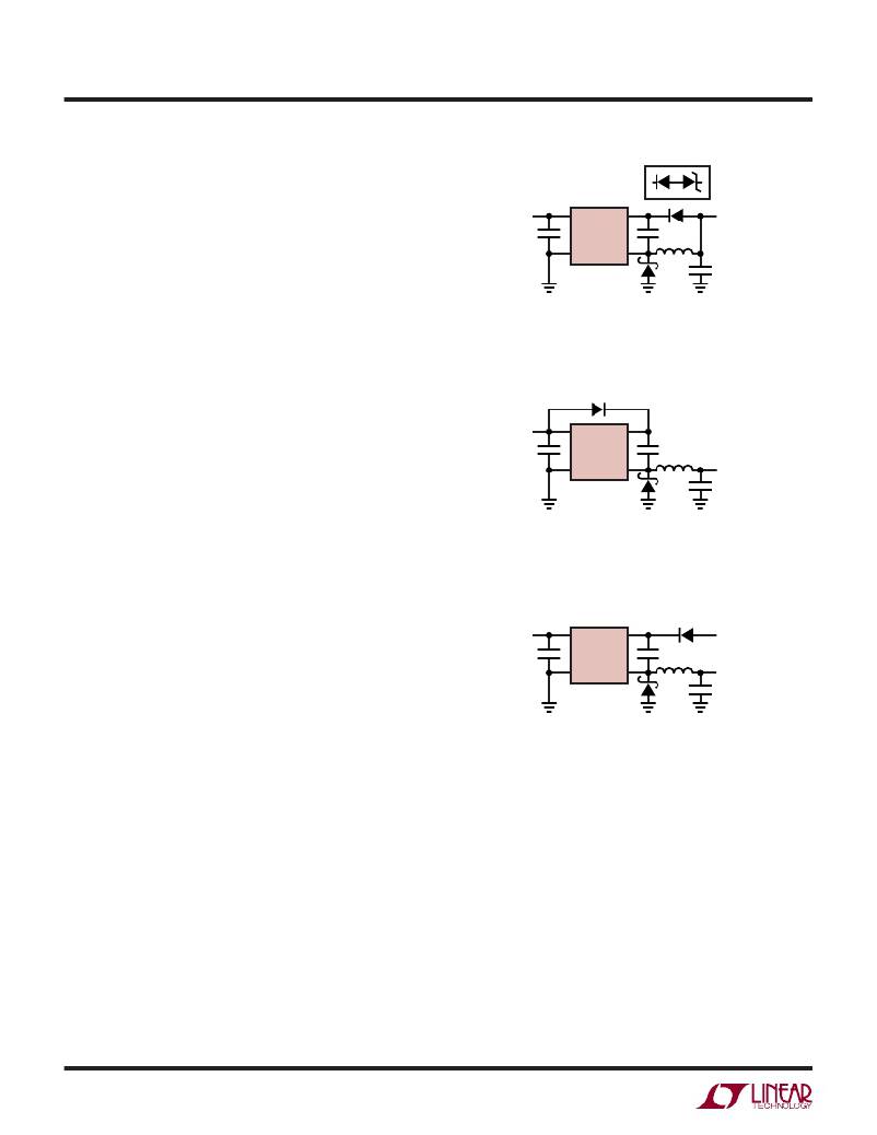
�BOOST� PIN�
�For� most� applications,� the� boost� components� are� a� 0.1� μ� F�
�capacitor� and� a� BAS21� diode.� The� anode� is� typically�
�(6b)�
�connected� to� the� regulated� output� voltage,� to� generate� a�
�voltage� approximately� V� OUT� above� V� IN� to� drive� the� output�
�stage� (Figure� 6a).� However,� the� output� stage� discharges�
�the� boost� capacitor� during� the� on� time� of� the� switch.� The�
�V� IN�
�V� IN� BOOST�
�LT3437�
�GND� SW�
�D� SS�
�V� DC�
�V� OUT�
�output� driver� requires� at� least� 2.5V� of� headroom� through-�
�out� this� period� to� keep� the� switch� fully� saturated.� If� the�
�output� voltage� is� less� than� 3.3V,� it� is� recommended� that� an�
�alternate� boost� supply� is� used.� The� boost� diode� can� be�
�connected� to� the� input� (Figure� 6b),� but� care� must� be� taken�
�to� prevent� the� boost� voltage� (V� BOOST� =� V� IN� ?� 2)� from�
�exceeding� the� BOOST� pin� absolute� maximum� rating.� The�
�additional� voltage� across� the� switch� driver� also� increases�
�power� loss� and� reduces� efficiency.� If� available,� an� inde-�
�pendent� supply� can� be� used� to� generate� the� required�
�BOOST� voltage� (Figure� 6c).� Tying� BOOST� to� V� IN� or� an�
�independent� supply� may� reduce� efficiency,� but� it� will�
�reduce� the� minimum� V� IN� required� to� start-up� with� light�
�loads.� If� the� generated� BOOST� voltage� dissipates� too�
�much� power� at� maximum� load,� the� BOOST� voltage� the�
�LT3437� sees� can� be� reduced� by� placing� a� Zener� diode� in�
�series� with� the� BOOST� diode� (Figure� 6a� option).�
�3437� F06�
�V� BOOST� –� V� SW� =� V� DC�
�V� BOOST(MAX)� =� V� DC� +� V� IN�
�(6c)�
�Figure� 6.� BOOST� Pin� Configurations�
�A� 0.1� μ� F� boost� capacitor� is� recommended� for� most� appli-�
�cations.� Almost� any� type� of� film� or� ceramic� capacitor� is�
�suitable,� but� the� ESR� should� be� <1� ?� to� ensure� it� can� be�
�fully� recharged� during� the� off� time� of� the� switch.� The�
�capacitor� value� is� derived� from� worst-case� conditions� of�
�4700ns� on� time,� 11mA� boost� current� and� 0.7V� discharge�
�ripple.� The� boost� capacitor� value� could� be� reduced� under�
�less� demanding� conditions,� but� this� will� not� improve�
�circuit� operation� or� efficiency.� Under� low� input� voltage� and�
�low� load� conditions,� a� higher� value� capacitor� will� reduce�
�discharge� ripple� and� improve� start-up� operation.�
�3437fc�
�18�
�相关PDF资料 |
PDF描述 |
|---|---|
| RBC19DREN-S734 | CONN EDGECARD 38POS .100 EYELET |
| ISC1812ER681J | INDUCTOR WW 680UH 5% 1812 |
| PM2120-221K | INDUCTOR TOROID 220UH 10% SMD |
| ISC1812ER471J | INDUCTOR WW 470UH 5% 1812 |
| LTC1751EMS8#PBF | IC REG SWITCHD CAP DBL ADJ 8MSOP |
相关代理商/技术参数 |
参数描述 |
|---|---|
| LT3437HFE | 制造商:LINER 制造商全称:Linear Technology 功能描述:High Voltage 500mA, 200kHz Step-Down Switching Regulator with 100μA Quiescent Current |
| LT3437HFE#PBF | 功能描述:IC REG BUCK ADJ 0.5A 16TSSOP RoHS:是 类别:集成电路 (IC) >> PMIC - 稳压器 - DC DC 开关稳压器 系列:- 标准包装:250 系列:- 类型:降压(降压) 输出类型:固定 输出数:1 输出电压:1.2V 输入电压:2.05 V ~ 6 V PWM 型:电压模式 频率 - 开关:2MHz 电流 - 输出:500mA 同步整流器:是 工作温度:-40°C ~ 85°C 安装类型:表面贴装 封装/外壳:6-UFDFN 包装:带卷 (TR) 供应商设备封装:6-SON(1.45x1) 产品目录页面:1032 (CN2011-ZH PDF) 其它名称:296-25628-2 |
| LT3437HFE#TRPBF | 功能描述:IC REG BUCK ADJ 0.5A 16TSSOP RoHS:是 类别:集成电路 (IC) >> PMIC - 稳压器 - DC DC 开关稳压器 系列:- 标准包装:2,500 系列:- 类型:降压(降压) 输出类型:固定 输出数:1 输出电压:1.2V,1.5V,1.8V,2.5V 输入电压:2.7 V ~ 20 V PWM 型:- 频率 - 开关:- 电流 - 输出:50mA 同步整流器:是 工作温度:-40°C ~ 125°C 安装类型:表面贴装 封装/外壳:10-TFSOP,10-MSOP(0.118",3.00mm 宽)裸露焊盘 包装:带卷 (TR) 供应商设备封装:10-MSOP 裸露焊盘 |
| LT3437IDD | 制造商:Linear Technology 功能描述:SP-SWREG/Monolithic, 60V, 500mA, 200kHz Step-down Converter w/ BurstMode |
| LT3437IDD#PBF | 功能描述:IC REG BUCK ADJ 0.5A 10DFN RoHS:是 类别:集成电路 (IC) >> PMIC - 稳压器 - DC DC 开关稳压器 系列:- 标准包装:250 系列:- 类型:降压(降压) 输出类型:固定 输出数:1 输出电压:1.2V 输入电压:2.05 V ~ 6 V PWM 型:电压模式 频率 - 开关:2MHz 电流 - 输出:500mA 同步整流器:是 工作温度:-40°C ~ 85°C 安装类型:表面贴装 封装/外壳:6-UFDFN 包装:带卷 (TR) 供应商设备封装:6-SON(1.45x1) 产品目录页面:1032 (CN2011-ZH PDF) 其它名称:296-25628-2 |
发布紧急采购,3分钟左右您将得到回复。