- 您现在的位置:买卖IC网 > PDF目录296330 > LTC2411CMS Analog-to-Digital Converter, 24-Bit PDF资料下载
参数资料
| 型号: | LTC2411CMS |
| 英文描述: | Analog-to-Digital Converter, 24-Bit |
| 中文描述: | 模拟到数字转换器,24比特 |
| 文件页数: | 11/40页 |
| 文件大小: | 450K |
| 代理商: | LTC2411CMS |
第1页第2页第3页第4页第5页第6页第7页第8页第9页第10页当前第11页第12页第13页第14页第15页第16页第17页第18页第19页第20页第21页第22页第23页第24页第25页第26页第27页第28页第29页第30页第31页第32页第33页第34页第35页第36页第37页第38页第39页第40页
LTC2411
19
In order to select the internal serial clock timing mode, the
serial clock pin (SCK) must be floating (Hi-Z) or pulled
HIGH prior to the falling edge of CS. The device will not
enter the internal serial clock mode if SCK is driven LOW
on the falling edge of CS. An internal weak pull-up resistor
is active on the SCK pin during the falling edge of CS;
therefore, the internal serial clock timing mode is auto-
matically selected if SCK is not externally driven.
The serial data output pin (SDO) is Hi-Z as long as CS is
HIGH. At any time during the conversion cycle, CS may be
pulled LOW in order to monitor the state of the converter.
Once CS is pulled LOW, SCK goes LOW and EOC is output
to the SDO pin. EOC = 1 while a conversion is in progress
and EOC = 0 if the device is in the sleep state.
When testing EOC, if the conversion is complete (EOC = 0),
the device will exit the sleep state and enter the data output
state if CS remains LOW. In order to prevent the device
from exiting the low power sleep state, CS must be pulled
HIGH before the first rising edge of SCK. In the internal
SCK timing mode, SCK goes HIGH and the device begins
outputting data at time tEOCtest after the falling edge of CS
(if EOC = 0) or tEOCtest after EOC goes LOW (if CS is LOW
during the falling edge of EOC). The value of tEOCtest is 23s
if the device is using its internal oscillator (F0 = logic LOW
or HIGH). If FO is driven by an external oscillator of
frequency fEOSC, then tEOCtest is 3.6/fEOSC. If CS is pulled
HIGH before time tEOCtest, the device remains in the sleep
state. The conversion result is held in the internal static
shift register.
If CS remains LOW longer than tEOCtest, the first rising
edge of SCK will occur and the conversion result is serially
shifted out of the SDO pin. The data output cycle begins on
this first rising edge of SCK and concludes after the 32nd
rising edge. Data is shifted out the SDO pin on each falling
edge of SCK. The internally generated serial clock is output
to the SCK pin. This signal may be used to shift the
conversion result into external circuitry. EOC can be
latched on the first rising edge of SCK and the last bit of the
conversion result on the 32nd rising edge of SCK. After the
32nd rising edge, SDO goes HIGH (EOC = 1), SCK stays
HIGH and a new conversion starts.
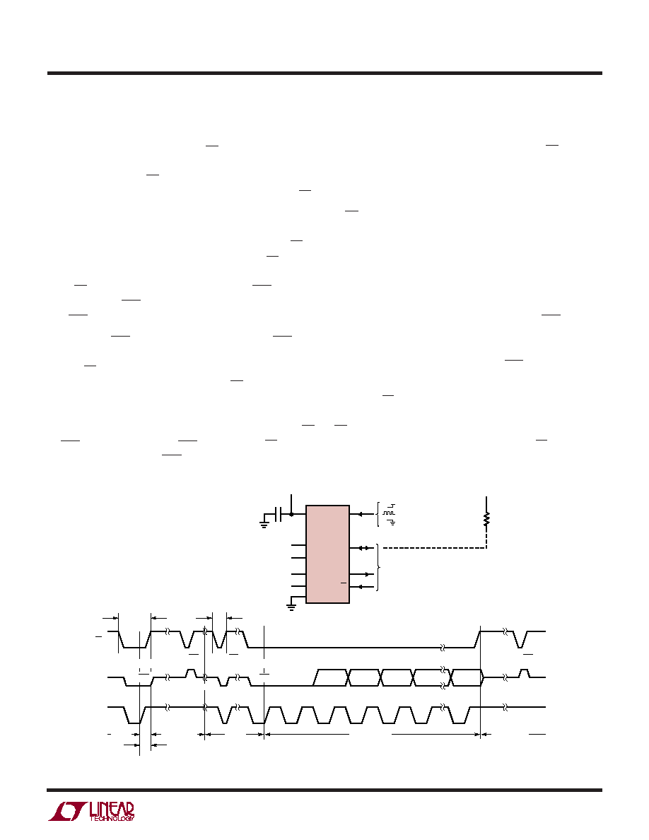
Typically, CS remains LOW during the data output state.
However, the data output state may be aborted by pulling
CS HIGH anytime between the first and 32nd rising edge
of SCK, see Figure 9. On the rising edge of CS, the device
aborts the data output state and immediately initiates a
Figure 9. Internal Serial Clock, Reduced Data Output Length
SDO
SCK
(INTERNAL)
CS
>tEOCtest
MSB
SIG
BIT 8
TEST EOC
BIT 27
BIT 26
BIT 28
BIT 29
BIT 30
EOC
BIT 31
EOC
BIT 0
SLEEP
DATA OUTPUT
Hi-Z
DATA OUTPUT
CONVERSION
SLEEP
2411 F09
<tEOCtest
VCC
10k
= 50Hz REJECTION
= EXTERNAL OSCILLATOR
= 60Hz REJECTION
VCC
TEST EOC
VCC
FO
REF+
REF–
SCK
IN+
IN–
SDO
GND
CS
110
2
3
9
4
5
8
6
7
REFERENCE
VOLTAGE
0.1V TO VCC
ANALOG INPUT RANGE
–0.5VREF TO 0.5VREF
3-WIRE
SPI INTERFACE
1
F
2.7V TO 5.5V
LTC2411
APPLICATIO S I FOR ATIO
WU
UU
相关PDF资料 |
PDF描述 |
|---|---|
| LTC3702SG | Optoelectronic |
| LTC3708SG | Optoelectronic |
| LTC3702SP | Optoelectronic |
| LTC3708SP | Optoelectronic |
| LTC3710E | Optoelectronic |
相关代理商/技术参数 |
参数描述 |
|---|---|
| LTC2411CMS#PBF | 功能描述:IC A/D CONV 24BIT MICRPWR 10MSOP RoHS:是 类别:集成电路 (IC) >> 数据采集 - 模数转换器 系列:- 标准包装:1 系列:microPOWER™ 位数:8 采样率(每秒):1M 数据接口:串行,SPI? 转换器数目:1 功率耗散(最大):- 电压电源:模拟和数字 工作温度:-40°C ~ 125°C 安装类型:表面贴装 封装/外壳:24-VFQFN 裸露焊盘 供应商设备封装:24-VQFN 裸露焊盘(4x4) 包装:Digi-Reel® 输入数目和类型:8 个单端,单极 产品目录页面:892 (CN2011-ZH PDF) 其它名称:296-25851-6 |
| LTC2411CMS#TR | 功能描述:IC A/D CONV 24BIT MICRPWR 10MSOP RoHS:否 类别:集成电路 (IC) >> 数据采集 - 模数转换器 系列:- 标准包装:1,000 系列:- 位数:16 采样率(每秒):45k 数据接口:串行 转换器数目:2 功率耗散(最大):315mW 电压电源:模拟和数字 工作温度:0°C ~ 70°C 安装类型:表面贴装 封装/外壳:28-SOIC(0.295",7.50mm 宽) 供应商设备封装:28-SOIC W 包装:带卷 (TR) 输入数目和类型:2 个单端,单极 |
| LTC2411CMS#TRPBF | 功能描述:IC A/D CONV 24BIT MICRPWR 10MSOP RoHS:是 类别:集成电路 (IC) >> 数据采集 - 模数转换器 系列:- 标准包装:1,000 系列:- 位数:16 采样率(每秒):45k 数据接口:串行 转换器数目:2 功率耗散(最大):315mW 电压电源:模拟和数字 工作温度:0°C ~ 70°C 安装类型:表面贴装 封装/外壳:28-SOIC(0.295",7.50mm 宽) 供应商设备封装:28-SOIC W 包装:带卷 (TR) 输入数目和类型:2 个单端,单极 |
| LTC2411IMS | 功能描述:IC A/D CONV 24BIT MICRPWR 10MSOP RoHS:否 类别:集成电路 (IC) >> 数据采集 - 模数转换器 系列:- 标准包装:1,000 系列:- 位数:16 采样率(每秒):45k 数据接口:串行 转换器数目:2 功率耗散(最大):315mW 电压电源:模拟和数字 工作温度:0°C ~ 70°C 安装类型:表面贴装 封装/外壳:28-SOIC(0.295",7.50mm 宽) 供应商设备封装:28-SOIC W 包装:带卷 (TR) 输入数目和类型:2 个单端,单极 |
| LTC2411IMS#PBF | 功能描述:IC A/D CONV 24BIT MICRPWR 10MSOP RoHS:是 类别:集成电路 (IC) >> 数据采集 - 模数转换器 系列:- 标准包装:1 系列:microPOWER™ 位数:8 采样率(每秒):1M 数据接口:串行,SPI? 转换器数目:1 功率耗散(最大):- 电压电源:模拟和数字 工作温度:-40°C ~ 125°C 安装类型:表面贴装 封装/外壳:24-VFQFN 裸露焊盘 供应商设备封装:24-VQFN 裸露焊盘(4x4) 包装:Digi-Reel® 输入数目和类型:8 个单端,单极 产品目录页面:892 (CN2011-ZH PDF) 其它名称:296-25851-6 |
发布紧急采购,3分钟左右您将得到回复。