- 您现在的位置:买卖IC网 > PDF目录296330 > LTC2411CMS Analog-to-Digital Converter, 24-Bit PDF资料下载
参数资料
| 型号: | LTC2411CMS |
| 英文描述: | Analog-to-Digital Converter, 24-Bit |
| 中文描述: | 模拟到数字转换器,24比特 |
| 文件页数: | 5/40页 |
| 文件大小: | 450K |
| 代理商: | LTC2411CMS |
第1页第2页第3页第4页当前第5页第6页第7页第8页第9页第10页第11页第12页第13页第14页第15页第16页第17页第18页第19页第20页第21页第22页第23页第24页第25页第26页第27页第28页第29页第30页第31页第32页第33页第34页第35页第36页第37页第38页第39页第40页
LTC2411
13
The function of these bits is summarized in Table 1.
Table 1. LTC2411 Status Bits
Bit 31
Bit 30 Bit 29 Bit 28
Input Range
EOC
DMY
SIG
MSB
VIN ≥ 0.5 VREF
00
1
0V
≤ VIN < 0.5 VREF
00
1
0
–0.5 VREF ≤ VIN < 0V
0
1
VIN < – 0.5 VREF
00
0
Bits 28-5 are the 24-bit conversion result MSB first.
Bit 5 is the least significant bit (LSB).
Bits 4-0 are sub LSBs below the 24-bit level. Bits 4-0 may
be included in averaging or discarded without loss of
resolution.
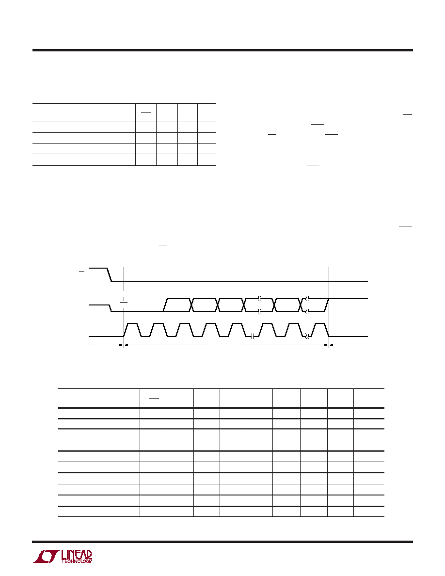
Data is shifted out of the SDO pin under control of the serial
clock (SCK), see Figure 3. Whenever CS is HIGH, SDO
remains high impedance and any externally generated
SCK clock pulses are ignored by the internal data out shift
register.
In order to shift the conversion result out of the device, CS
must first be driven LOW. EOC is seen at the SDO pin of the
device once CS is pulled LOW. EOC changes real time from
HIGH to LOW at the completion of a conversion. This
signal may be used as an interrupt for an external
microcontroller. Bit 31 (EOC) can be captured on the first
rising edge of SCK. Bit 30 is shifted out of the device on the
first falling edge of SCK. The final data bit (Bit 0) is shifted
out on the falling edge of the 31st SCK and may be latched
on the rising edge of the 32nd SCK pulse. On the falling
edge of the 32nd SCK pulse, SDO goes HIGH indicating the
initiation of a new conversion cycle. This bit serves as EOC
(Bit 31) for the next conversion cycle. Table 2 summarizes
the output data format.
Table 2. LTC2411 Output Data Format
Differential Input Voltage
Bit 31
Bit 30
Bit 29
Bit 28
Bit 27
Bit 26
Bit 25
…
Bit 0
VIN*
EOC
DMY
SIG
MSB
VIN* ≥ 0.5 VREF**
0
0110
0
…
0
0.5 VREF** – 1LSB
0
0101
1
…
1
0.25 VREF**
0
0101
0
…
0
0.25 VREF** – 1LSB
0
0100
1
…
1
0
0100
0
…
0
–1LSB
0
0011
1
…
1
– 0.25 VREF**
0
0011
0
…
0
– 0.25 VREF** – 1LSB
0
0010
1
…
1
– 0.5 VREF**
0
0010
0
…
0
VIN* < –0.5 VREF**
0
0001
1
…
1
*The differential input voltage VIN = IN+ – IN–.
**The differential reference voltage VREF = REF+ – REF–.
Figure 3. Output Data Timing
MSB
SIG
“0”
1
2
3
4
5
262732
BIT 0
BIT 27
BIT 5
LSB24
BIT 28
BIT 29
BIT 30
SDO
SCK
CS
EOC
BIT 31
SLEEP
DATA OUTPUT
CONVERSION
2411 F03
Hi-Z
APPLICATIO S I FOR ATIO
WU
UU
相关PDF资料 |
PDF描述 |
|---|---|
| LTC3702SG | Optoelectronic |
| LTC3708SG | Optoelectronic |
| LTC3702SP | Optoelectronic |
| LTC3708SP | Optoelectronic |
| LTC3710E | Optoelectronic |
相关代理商/技术参数 |
参数描述 |
|---|---|
| LTC2411CMS#PBF | 功能描述:IC A/D CONV 24BIT MICRPWR 10MSOP RoHS:是 类别:集成电路 (IC) >> 数据采集 - 模数转换器 系列:- 标准包装:1 系列:microPOWER™ 位数:8 采样率(每秒):1M 数据接口:串行,SPI? 转换器数目:1 功率耗散(最大):- 电压电源:模拟和数字 工作温度:-40°C ~ 125°C 安装类型:表面贴装 封装/外壳:24-VFQFN 裸露焊盘 供应商设备封装:24-VQFN 裸露焊盘(4x4) 包装:Digi-Reel® 输入数目和类型:8 个单端,单极 产品目录页面:892 (CN2011-ZH PDF) 其它名称:296-25851-6 |
| LTC2411CMS#TR | 功能描述:IC A/D CONV 24BIT MICRPWR 10MSOP RoHS:否 类别:集成电路 (IC) >> 数据采集 - 模数转换器 系列:- 标准包装:1,000 系列:- 位数:16 采样率(每秒):45k 数据接口:串行 转换器数目:2 功率耗散(最大):315mW 电压电源:模拟和数字 工作温度:0°C ~ 70°C 安装类型:表面贴装 封装/外壳:28-SOIC(0.295",7.50mm 宽) 供应商设备封装:28-SOIC W 包装:带卷 (TR) 输入数目和类型:2 个单端,单极 |
| LTC2411CMS#TRPBF | 功能描述:IC A/D CONV 24BIT MICRPWR 10MSOP RoHS:是 类别:集成电路 (IC) >> 数据采集 - 模数转换器 系列:- 标准包装:1,000 系列:- 位数:16 采样率(每秒):45k 数据接口:串行 转换器数目:2 功率耗散(最大):315mW 电压电源:模拟和数字 工作温度:0°C ~ 70°C 安装类型:表面贴装 封装/外壳:28-SOIC(0.295",7.50mm 宽) 供应商设备封装:28-SOIC W 包装:带卷 (TR) 输入数目和类型:2 个单端,单极 |
| LTC2411IMS | 功能描述:IC A/D CONV 24BIT MICRPWR 10MSOP RoHS:否 类别:集成电路 (IC) >> 数据采集 - 模数转换器 系列:- 标准包装:1,000 系列:- 位数:16 采样率(每秒):45k 数据接口:串行 转换器数目:2 功率耗散(最大):315mW 电压电源:模拟和数字 工作温度:0°C ~ 70°C 安装类型:表面贴装 封装/外壳:28-SOIC(0.295",7.50mm 宽) 供应商设备封装:28-SOIC W 包装:带卷 (TR) 输入数目和类型:2 个单端,单极 |
| LTC2411IMS#PBF | 功能描述:IC A/D CONV 24BIT MICRPWR 10MSOP RoHS:是 类别:集成电路 (IC) >> 数据采集 - 模数转换器 系列:- 标准包装:1 系列:microPOWER™ 位数:8 采样率(每秒):1M 数据接口:串行,SPI? 转换器数目:1 功率耗散(最大):- 电压电源:模拟和数字 工作温度:-40°C ~ 125°C 安装类型:表面贴装 封装/外壳:24-VFQFN 裸露焊盘 供应商设备封装:24-VQFN 裸露焊盘(4x4) 包装:Digi-Reel® 输入数目和类型:8 个单端,单极 产品目录页面:892 (CN2011-ZH PDF) 其它名称:296-25851-6 |
发布紧急采购,3分钟左右您将得到回复。