- 您现在的位置:买卖IC网 > PDF目录10302 > LTC2412IGN#TR (Linear Technology)IC CONV A/D 24B 2CH DIFF 16-SSOP PDF资料下载
参数资料
| 型号: | LTC2412IGN#TR |
| 厂商: | Linear Technology |
| 文件页数: | 17/36页 |
| 文件大小: | 0K |
| 描述: | IC CONV A/D 24B 2CH DIFF 16-SSOP |
| 标准包装: | 2,500 |
| 位数: | 24 |
| 采样率(每秒): | 7.5 |
| 数据接口: | MICROWIRE?,串行,SPI? |
| 转换器数目: | 1 |
| 功率耗散(最大): | 1mW |
| 电压电源: | 单电源 |
| 工作温度: | -40°C ~ 85°C |
| 安装类型: | 表面贴装 |
| 封装/外壳: | 16-SSOP(0.154",3.90mm 宽) |
| 供应商设备封装: | 16-SSOP |
| 包装: | 带卷 (TR) |
| 输入数目和类型: | 1 个差分,双极 |
| 配用: | DC746A-ND - BOARD DELTA SIGMA ADC LTC2412 |
第1页第2页第3页第4页第5页第6页第7页第8页第9页第10页第11页第12页第13页第14页第15页第16页当前第17页第18页第19页第20页第21页第22页第23页第24页第25页第26页第27页第28页第29页第30页第31页第32页第33页第34页第35页第36页
LTC2412
24
2412f
APPLICATIO S I FOR ATIO
WU
U
For a simple approximation, the source impedance RS
driving an analog input pin (IN+, IN–, REF+ or REF–) can be
considered to form, together with RSW and CEQ (see
Figure 11), a first order passive network with a time
constant
τ = (RS + RSW) CEQ. The converter is able to
sample the input signal with better than 1ppm accuracy if
the sampling period is at least 14 times greater than the
input circuit time constant
τ. The sampling process on the
four input analog pins is quasi-independent so each time
constant should be considered by itself and, under worst-
case circumstances, the errors may add.
When using the internal oscillator (FO = LOW or HIGH), the
LTC2412’s front-end switched-capacitor network is clocked
at 76800Hz corresponding to a 13
s sampling period.
Thus, for settling errors of less than 1ppm, the driving
source impedance should be chosen such that
τ≤13s/14
= 920ns. When an external oscillator of frequency fEOSC is
used, the sampling period is 2/fEOSC and, for a settling
error of less than 1ppm,
τ ≤ 0.14/fEOSC.
Input Current
If complete settling occurs on the input, conversion re-
sults will be unaffected by the dynamic input current. An
incomplete settling of the input signal sampling process
may result in gain and offset errors, but it will not degrade
the INL performance of the converter. Figure 11 shows the
mathematical expressions for the average bias currents
flowing through the IN+ and IN– pins as a result of the
sampling charge transfers when integrated over a sub-
stantial time period (longer than 64 internal clock cycles).
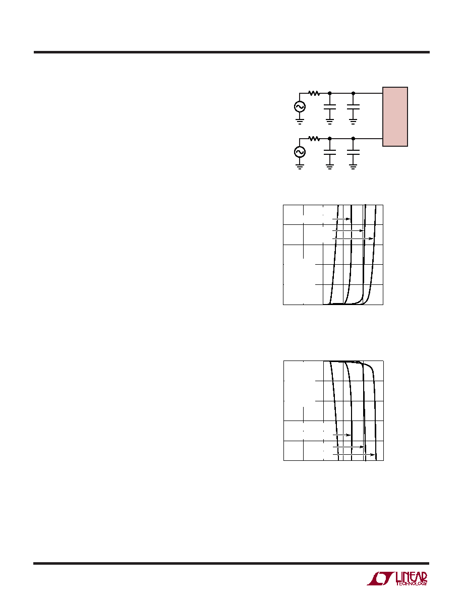
The effect of this input dynamic current can be analyzed
using the test circuit of Figure 12. The CPAR capacitor
includes the LTC2412 pin capacitance (5pF typical) plus
the capacitance of the test fixture used to obtain the results
shown in Figures 13 and 14. A careful implementation can
bring the total input capacitance (CIN + CPAR) closer to 5pF
thus achieving better performance than the one predicted
by Figures 13 and 14. For simplicity, two distinct situa-
tions can be considered.
For relatively small values of input capacitance (CIN <
0.01
F), the voltage on the sampling capacitor settles
almost completely and relatively large values for the
source impedance result in only small errors. Such values
CIN
2412 F12
VINCM + 0.5VIN
RSOURCE
IN+
LTC2412
CPAR
20pF
CIN
VINCM – 0.5VIN
RSOURCE
IN –
CPAR
20pF
Figure 12. An RC Network at IN+ and IN–
Figure 14. –FS Error vs RSOURCE at IN+ or IN– (Small CIN)
Figure 13. +FS Error vs RSOURCE at IN+ or IN– (Small CIN)
RSOURCE ()
1
10
100
1k
10k
100k
+FS
ERROR
(ppm
OF
V
REF
)
2412 F13
50
40
30
20
10
0
VCC = 5V
REF+ = 5V
REF – = GND
IN+ = 5V
IN– = 2.5V
FO = GND
TA = 25°C
CIN = 0.01F
CIN = 0.001F
CIN = 100pF
CIN = 0pF
RSOURCE ()
1
10
100
1k
10k
100k
–
FS
ERROR
(ppm
OF
V
REF
)
2412 F14
0
–10
–20
–30
–40
–50
VCC = 5V
REF+ = 5V
REF – = GND
IN+ = GND
IN– = 2.5V
FO = GND
TA = 25°C
CIN = 0.01F
CIN = 0.001F
CIN = 100pF
CIN = 0pF
for CIN will deteriorate the converter offset and gain
performance without significant benefits of signal filtering
and the user is advised to avoid them. Nevertheless, when
small values of CIN are unavoidably present as parasitics
相关PDF资料 |
PDF描述 |
|---|---|
| AD7401YRWZ-REEL7 | IC MODULATOR SIGMA-DELTA 16SOIC |
| VE-BTZ-MV-S | CONVERTER MOD DC/DC 2V 60W |
| AD7924WYRUZ-REEL7 | IC ADC 12BIT 4CH W/SEQ 16TSSOP |
| VE-BTX-MW-S | CONVERTER MOD DC/DC 5.2V 100W |
| AD7705BRU-REEL | IC ADC 16BIT 2CH 16-TSSOP T/R |
相关代理商/技术参数 |
参数描述 |
|---|---|
| LTC2413CGN | 功能描述:IC A/D CONV 24BIT MICRPWR 16SSOP RoHS:否 类别:集成电路 (IC) >> 数据采集 - 模数转换器 系列:- 标准包装:1,000 系列:- 位数:16 采样率(每秒):45k 数据接口:串行 转换器数目:2 功率耗散(最大):315mW 电压电源:模拟和数字 工作温度:0°C ~ 70°C 安装类型:表面贴装 封装/外壳:28-SOIC(0.295",7.50mm 宽) 供应商设备封装:28-SOIC W 包装:带卷 (TR) 输入数目和类型:2 个单端,单极 |
| LTC2413CGN#PBF | 功能描述:IC A/D CONV 24BIT MICRPWR 16SSOP RoHS:是 类别:集成电路 (IC) >> 数据采集 - 模数转换器 系列:- 标准包装:1 系列:microPOWER™ 位数:8 采样率(每秒):1M 数据接口:串行,SPI? 转换器数目:1 功率耗散(最大):- 电压电源:模拟和数字 工作温度:-40°C ~ 125°C 安装类型:表面贴装 封装/外壳:24-VFQFN 裸露焊盘 供应商设备封装:24-VQFN 裸露焊盘(4x4) 包装:Digi-Reel® 输入数目和类型:8 个单端,单极 产品目录页面:892 (CN2011-ZH PDF) 其它名称:296-25851-6 |
| LTC2413CGN#TR | 功能描述:IC ADC 24BIT 50/60HZ MPWR 16SSOP RoHS:否 类别:集成电路 (IC) >> 数据采集 - 模数转换器 系列:- 标准包装:1,000 系列:- 位数:16 采样率(每秒):45k 数据接口:串行 转换器数目:2 功率耗散(最大):315mW 电压电源:模拟和数字 工作温度:0°C ~ 70°C 安装类型:表面贴装 封装/外壳:28-SOIC(0.295",7.50mm 宽) 供应商设备封装:28-SOIC W 包装:带卷 (TR) 输入数目和类型:2 个单端,单极 |
| LTC2413CGN#TRPBF | 功能描述:IC A/D CONV 24BIT MICRPWR 16SSOP RoHS:是 类别:集成电路 (IC) >> 数据采集 - 模数转换器 系列:- 标准包装:1,000 系列:- 位数:16 采样率(每秒):45k 数据接口:串行 转换器数目:2 功率耗散(最大):315mW 电压电源:模拟和数字 工作温度:0°C ~ 70°C 安装类型:表面贴装 封装/外壳:28-SOIC(0.295",7.50mm 宽) 供应商设备封装:28-SOIC W 包装:带卷 (TR) 输入数目和类型:2 个单端,单极 |
| LTC2413IGN | 功能描述:IC A/D CONV 24BIT MICRPWR 16SSOP RoHS:否 类别:集成电路 (IC) >> 数据采集 - 模数转换器 系列:- 标准包装:1,000 系列:- 位数:16 采样率(每秒):45k 数据接口:串行 转换器数目:2 功率耗散(最大):315mW 电压电源:模拟和数字 工作温度:0°C ~ 70°C 安装类型:表面贴装 封装/外壳:28-SOIC(0.295",7.50mm 宽) 供应商设备封装:28-SOIC W 包装:带卷 (TR) 输入数目和类型:2 个单端,单极 |
发布紧急采购,3分钟左右您将得到回复。