- 您现在的位置:买卖IC网 > PDF目录10302 > LTC2412IGN#TR (Linear Technology)IC CONV A/D 24B 2CH DIFF 16-SSOP PDF资料下载
参数资料
| 型号: | LTC2412IGN#TR |
| 厂商: | Linear Technology |
| 文件页数: | 24/36页 |
| 文件大小: | 0K |
| 描述: | IC CONV A/D 24B 2CH DIFF 16-SSOP |
| 标准包装: | 2,500 |
| 位数: | 24 |
| 采样率(每秒): | 7.5 |
| 数据接口: | MICROWIRE?,串行,SPI? |
| 转换器数目: | 1 |
| 功率耗散(最大): | 1mW |
| 电压电源: | 单电源 |
| 工作温度: | -40°C ~ 85°C |
| 安装类型: | 表面贴装 |
| 封装/外壳: | 16-SSOP(0.154",3.90mm 宽) |
| 供应商设备封装: | 16-SSOP |
| 包装: | 带卷 (TR) |
| 输入数目和类型: | 1 个差分,双极 |
| 配用: | DC746A-ND - BOARD DELTA SIGMA ADC LTC2412 |
第1页第2页第3页第4页第5页第6页第7页第8页第9页第10页第11页第12页第13页第14页第15页第16页第17页第18页第19页第20页第21页第22页第23页当前第24页第25页第26页第27页第28页第29页第30页第31页第32页第33页第34页第35页第36页
LTC2412
30
2412f
APPLICATIO S I FOR ATIO
WU
U
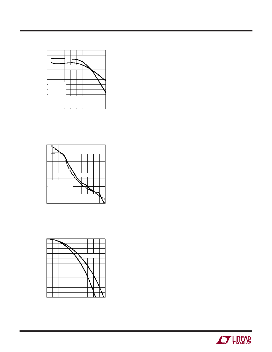
Input Bandwidth
The combined effect of the internal Sinc4 digital filter and
of the analog and digital autocalibration circuits deter-
mines the LTC2412 input bandwidth. When the internal
oscillator is used with the notch set at 60Hz (FO = LOW),
the 3dB input bandwidth is 3.63Hz. When the internal
oscillator is used with the notch set at 50Hz (FO = HIGH),
the 3dB input bandwidth is 3.02Hz. If an external conver-
sion clock generator of frequency fEOSC is connected to the
FO pin, the 3dB input bandwidth is 0.236 10–6 fEOSC.
Due to the complex filtering and calibration algorithms
utilized, the converter input bandwidth is not modeled very
accurately by a first order filter with the pole located at the
3dB frequency. When the internal oscillator is used, the
shape of the LTC2412 input bandwidth is shown in Fig-
ure 31 for FO = LOW and FO = HIGH. When an external
oscillator of frequency fEOSC is used, the shape of the
LTC2412 input bandwidth can be derived from Figure 31,
FO = LOW curve in which the horizontal axis is scaled by
fEOSC/153600.
The conversion noise (800nVRMS typical for VREF = 5V)
can be modeled by a white noise source connected to a
noise free converter. The noise spectral density is
62.75nV/
√Hz for an infinite bandwidth source and
86.1nV/
√Hz for a single 0.5MHz pole source. From these
numbers, it is clear that particular attention must be given
to the design of external amplification circuits. Such
circuits face the simultaneous requirements of very low
bandwidth (just a few Hz) in order to reduce the output
referred noise and relatively high bandwidth (at least
500kHz) necessary to drive the input switched-capacitor
network. A possible solution is a high gain, low bandwidth
amplifier stage followed by a high bandwidth unity-gain
buffer.
When external amplifiers are driving the LTC2412, the
ADC input referred system noise calculation can be simpli-
fied by Figure 32. The noise of an amplifier driving the
LTC2412 input pin can be modeled as a band limited white
noise source. Its bandwidth can be approximated by the
bandwidth of a single pole lowpass filter with a corner
frequency fi. The amplifier noise spectral density is ni.
From Figure 32, using fi as the x-axis selector, we can find
on the y-axis the noise equivalent bandwidth freqi of the
Figure 29. Resolution (NoiseRMS ≤ 1LSB)
vs Output Data Rate and Reference Voltage
Figure 30. Resolution (INLMAX ≤ 1LSB)
vs Output Data Rate and Reference Voltage
Figure 31. Input Signal Bandwidth
Using the Internal Oscillator
OUTPUT DATA RATE (READINGS/SEC)
0
102030405060708090 100
RESOLUTION
(BITS)
2412 F29
24
23
22
21
20
19
18
17
16
15
14
13
12
VREF = 5V
VCC = 5V
REF – = GND
VINCM = 2.5V
VIN = 0V
FO = EXTERNAL OSCILLATOR
TA = 25°C
RESOLUTION = LOG2(VREF/NOISERMS)
VREF = 2.5V
OUTPUT DATA RATE (READINGS/SEC)
0
102030405060708090 100
RESOLUTION
(BITS)
2412 F30
22
20
18
16
14
12
10
8
TA = 25°C
VCC = 5V
REF – = GND
VINCM = 0.5 REF
+
–0.5V VREF < VIN < 0.5 VREF
FO = EXTERNAL OSCILLATOR
VREF = 2.5V
VREF = 5V
RESOLUTION =
LOG2(VREF/INLMAX)
DIFFERENTIAL INPUT SIGNAL FREQUENCY (Hz)
0
0.5
1
1.5
2
2.5
3
3.5
4
4.5
5
INPUT
SIGNAL
ATTENUATION
(dB)
2412 F31
0.0
–0.5
–1.0
–1.5
–2.0
–2.5
–3.0
–3.5
–4.0
–4.5
–5.0
–5.5
–6.0
FO = HIGH
FO = LOW
相关PDF资料 |
PDF描述 |
|---|---|
| AD7401YRWZ-REEL7 | IC MODULATOR SIGMA-DELTA 16SOIC |
| VE-BTZ-MV-S | CONVERTER MOD DC/DC 2V 60W |
| AD7924WYRUZ-REEL7 | IC ADC 12BIT 4CH W/SEQ 16TSSOP |
| VE-BTX-MW-S | CONVERTER MOD DC/DC 5.2V 100W |
| AD7705BRU-REEL | IC ADC 16BIT 2CH 16-TSSOP T/R |
相关代理商/技术参数 |
参数描述 |
|---|---|
| LTC2413CGN | 功能描述:IC A/D CONV 24BIT MICRPWR 16SSOP RoHS:否 类别:集成电路 (IC) >> 数据采集 - 模数转换器 系列:- 标准包装:1,000 系列:- 位数:16 采样率(每秒):45k 数据接口:串行 转换器数目:2 功率耗散(最大):315mW 电压电源:模拟和数字 工作温度:0°C ~ 70°C 安装类型:表面贴装 封装/外壳:28-SOIC(0.295",7.50mm 宽) 供应商设备封装:28-SOIC W 包装:带卷 (TR) 输入数目和类型:2 个单端,单极 |
| LTC2413CGN#PBF | 功能描述:IC A/D CONV 24BIT MICRPWR 16SSOP RoHS:是 类别:集成电路 (IC) >> 数据采集 - 模数转换器 系列:- 标准包装:1 系列:microPOWER™ 位数:8 采样率(每秒):1M 数据接口:串行,SPI? 转换器数目:1 功率耗散(最大):- 电压电源:模拟和数字 工作温度:-40°C ~ 125°C 安装类型:表面贴装 封装/外壳:24-VFQFN 裸露焊盘 供应商设备封装:24-VQFN 裸露焊盘(4x4) 包装:Digi-Reel® 输入数目和类型:8 个单端,单极 产品目录页面:892 (CN2011-ZH PDF) 其它名称:296-25851-6 |
| LTC2413CGN#TR | 功能描述:IC ADC 24BIT 50/60HZ MPWR 16SSOP RoHS:否 类别:集成电路 (IC) >> 数据采集 - 模数转换器 系列:- 标准包装:1,000 系列:- 位数:16 采样率(每秒):45k 数据接口:串行 转换器数目:2 功率耗散(最大):315mW 电压电源:模拟和数字 工作温度:0°C ~ 70°C 安装类型:表面贴装 封装/外壳:28-SOIC(0.295",7.50mm 宽) 供应商设备封装:28-SOIC W 包装:带卷 (TR) 输入数目和类型:2 个单端,单极 |
| LTC2413CGN#TRPBF | 功能描述:IC A/D CONV 24BIT MICRPWR 16SSOP RoHS:是 类别:集成电路 (IC) >> 数据采集 - 模数转换器 系列:- 标准包装:1,000 系列:- 位数:16 采样率(每秒):45k 数据接口:串行 转换器数目:2 功率耗散(最大):315mW 电压电源:模拟和数字 工作温度:0°C ~ 70°C 安装类型:表面贴装 封装/外壳:28-SOIC(0.295",7.50mm 宽) 供应商设备封装:28-SOIC W 包装:带卷 (TR) 输入数目和类型:2 个单端,单极 |
| LTC2413IGN | 功能描述:IC A/D CONV 24BIT MICRPWR 16SSOP RoHS:否 类别:集成电路 (IC) >> 数据采集 - 模数转换器 系列:- 标准包装:1,000 系列:- 位数:16 采样率(每秒):45k 数据接口:串行 转换器数目:2 功率耗散(最大):315mW 电压电源:模拟和数字 工作温度:0°C ~ 70°C 安装类型:表面贴装 封装/外壳:28-SOIC(0.295",7.50mm 宽) 供应商设备封装:28-SOIC W 包装:带卷 (TR) 输入数目和类型:2 个单端,单极 |
发布紧急采购,3分钟左右您将得到回复。