- 您现在的位置:买卖IC网 > PDF目录10302 > LTC2412IGN#TR (Linear Technology)IC CONV A/D 24B 2CH DIFF 16-SSOP PDF资料下载
参数资料
| 型号: | LTC2412IGN#TR |
| 厂商: | Linear Technology |
| 文件页数: | 8/36页 |
| 文件大小: | 0K |
| 描述: | IC CONV A/D 24B 2CH DIFF 16-SSOP |
| 标准包装: | 2,500 |
| 位数: | 24 |
| 采样率(每秒): | 7.5 |
| 数据接口: | MICROWIRE?,串行,SPI? |
| 转换器数目: | 1 |
| 功率耗散(最大): | 1mW |
| 电压电源: | 单电源 |
| 工作温度: | -40°C ~ 85°C |
| 安装类型: | 表面贴装 |
| 封装/外壳: | 16-SSOP(0.154",3.90mm 宽) |
| 供应商设备封装: | 16-SSOP |
| 包装: | 带卷 (TR) |
| 输入数目和类型: | 1 个差分,双极 |
| 配用: | DC746A-ND - BOARD DELTA SIGMA ADC LTC2412 |
第1页第2页第3页第4页第5页第6页第7页当前第8页第9页第10页第11页第12页第13页第14页第15页第16页第17页第18页第19页第20页第21页第22页第23页第24页第25页第26页第27页第28页第29页第30页第31页第32页第33页第34页第35页第36页
LTC2412
16
2412f
APPLICATIO S I FOR ATIO
WU
U
outside specifications but the following conversions will
not be affected. If the change occurs during the data output
state and the converter is in the Internal SCK mode, the
serial clock duty cycle may be affected but the serial data
stream will remain valid.
Table 3 summarizes the duration of each state and the
achievable output data rate as a function of FO.
SERIAL INTERFACE PINS
The LTC2412 transmits the conversion results and re-
ceives the start of conversion command through a syn-
chronous 3-wire interface. During the conversion and
sleep states, this interface can be used to assess the
converter status and during the data output state it is used
to read the conversion result.
Serial Clock Input/Output (SCK)
The serial clock signal present on SCK (Pin 13) is used to
synchronize the data transfer. Each bit of data is shifted out
the SDO pin on the falling edge of the serial clock.
In the Internal SCK mode of operation, the SCK pin is an
output and the LTC2412 creates its own serial clock by
dividing the internal conversion clock by 8. In the External
SCK mode of operation, the SCK pin is used as input. The
internal or external SCK mode is selected on power-up and
then reselected every time a HIGH-to-LOW transition is
detected at the CS pin. If SCK is HIGH or floating at power-
up or during this transition, the converter enters the inter-
nal SCK mode. If SCK is LOW at power-up or during this
transition, the converter enters the external SCK mode.
Serial Data Output (SDO)
The serial data output pin, SDO (Pin 12), provides the
result of the last conversion as a serial bit stream (MSB
first) during the data output state. In addition, the SDO pin
is used as an end of conversion indicator during the
conversion and sleep states.
When CS (Pin 11) is HIGH, the SDO driver is switched to
a high impedance state. This allows sharing the serial
interface with other devices. If CS is LOW during the
convert or sleep state, SDO will output EOC. If CS is LOW
during the conversion phase, the EOC bit appears HIGH on
the SDO pin. Once the conversion is complete, EOC goes
LOW.
Chip Select Input (CS)
The active LOW chip select, CS (Pin 11), is used to test the
conversion status and to enable the data output transfer as
described in the previous sections.
In addition, the CS signal can be used to trigger a new
conversion cycle before the entire serial data transfer has
been completed. The LTC2412 will abort any serial data
transfer in progress and start a new conversion cycle
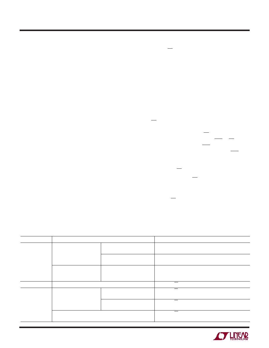
Table 3. LTC2412 State Duration
State
Operating Mode
Duration
CONVERT
Internal Oscillator
FO = LOW
133ms, Output Data Rate
≤ 7.5 Readings/s
(60Hz Rejection)
FO = HIGH
160ms, Output Data Rate
≤ 6.2 Readings/s
(50Hz Rejection)
External Oscillator
FO = External Oscillator
20510/fEOSCs, Output Data Rate ≤ fEOSC/20510 Readings/s
with Frequency fEOSC kHz
(fEOSC/2560 Rejection)
SLEEP
As Long As CS = HIGH
DATA OUTPUT
Internal Serial Clock
FO = LOW/HIGH
As Long As CS = LOW But Not Longer Than 1.67ms
(Internal Oscillator)
(32 SCK cycles)
FO = External Oscillator with
As Long As CS = LOW But Not Longer Than 256/fEOSCms
Frequency fEOSC kHz
(32 SCK cycles)
External Serial Clock with
As Long As CS = LOW But Not Longer Than 32/fSCKms
Frequency fSCK kHz
(32 SCK cycles)
相关PDF资料 |
PDF描述 |
|---|---|
| AD7401YRWZ-REEL7 | IC MODULATOR SIGMA-DELTA 16SOIC |
| VE-BTZ-MV-S | CONVERTER MOD DC/DC 2V 60W |
| AD7924WYRUZ-REEL7 | IC ADC 12BIT 4CH W/SEQ 16TSSOP |
| VE-BTX-MW-S | CONVERTER MOD DC/DC 5.2V 100W |
| AD7705BRU-REEL | IC ADC 16BIT 2CH 16-TSSOP T/R |
相关代理商/技术参数 |
参数描述 |
|---|---|
| LTC2413CGN | 功能描述:IC A/D CONV 24BIT MICRPWR 16SSOP RoHS:否 类别:集成电路 (IC) >> 数据采集 - 模数转换器 系列:- 标准包装:1,000 系列:- 位数:16 采样率(每秒):45k 数据接口:串行 转换器数目:2 功率耗散(最大):315mW 电压电源:模拟和数字 工作温度:0°C ~ 70°C 安装类型:表面贴装 封装/外壳:28-SOIC(0.295",7.50mm 宽) 供应商设备封装:28-SOIC W 包装:带卷 (TR) 输入数目和类型:2 个单端,单极 |
| LTC2413CGN#PBF | 功能描述:IC A/D CONV 24BIT MICRPWR 16SSOP RoHS:是 类别:集成电路 (IC) >> 数据采集 - 模数转换器 系列:- 标准包装:1 系列:microPOWER™ 位数:8 采样率(每秒):1M 数据接口:串行,SPI? 转换器数目:1 功率耗散(最大):- 电压电源:模拟和数字 工作温度:-40°C ~ 125°C 安装类型:表面贴装 封装/外壳:24-VFQFN 裸露焊盘 供应商设备封装:24-VQFN 裸露焊盘(4x4) 包装:Digi-Reel® 输入数目和类型:8 个单端,单极 产品目录页面:892 (CN2011-ZH PDF) 其它名称:296-25851-6 |
| LTC2413CGN#TR | 功能描述:IC ADC 24BIT 50/60HZ MPWR 16SSOP RoHS:否 类别:集成电路 (IC) >> 数据采集 - 模数转换器 系列:- 标准包装:1,000 系列:- 位数:16 采样率(每秒):45k 数据接口:串行 转换器数目:2 功率耗散(最大):315mW 电压电源:模拟和数字 工作温度:0°C ~ 70°C 安装类型:表面贴装 封装/外壳:28-SOIC(0.295",7.50mm 宽) 供应商设备封装:28-SOIC W 包装:带卷 (TR) 输入数目和类型:2 个单端,单极 |
| LTC2413CGN#TRPBF | 功能描述:IC A/D CONV 24BIT MICRPWR 16SSOP RoHS:是 类别:集成电路 (IC) >> 数据采集 - 模数转换器 系列:- 标准包装:1,000 系列:- 位数:16 采样率(每秒):45k 数据接口:串行 转换器数目:2 功率耗散(最大):315mW 电压电源:模拟和数字 工作温度:0°C ~ 70°C 安装类型:表面贴装 封装/外壳:28-SOIC(0.295",7.50mm 宽) 供应商设备封装:28-SOIC W 包装:带卷 (TR) 输入数目和类型:2 个单端,单极 |
| LTC2413IGN | 功能描述:IC A/D CONV 24BIT MICRPWR 16SSOP RoHS:否 类别:集成电路 (IC) >> 数据采集 - 模数转换器 系列:- 标准包装:1,000 系列:- 位数:16 采样率(每秒):45k 数据接口:串行 转换器数目:2 功率耗散(最大):315mW 电压电源:模拟和数字 工作温度:0°C ~ 70°C 安装类型:表面贴装 封装/外壳:28-SOIC(0.295",7.50mm 宽) 供应商设备封装:28-SOIC W 包装:带卷 (TR) 输入数目和类型:2 个单端,单极 |
发布紧急采购,3分钟左右您将得到回复。