- 您现在的位置:买卖IC网 > PDF目录67761 > M34519M8-XXXFP 4-BIT, MROM, 6 MHz, MICROCONTROLLER, PDSO42 PDF资料下载
参数资料
| 型号: | M34519M8-XXXFP |
| 元件分类: | 微控制器/微处理器 |
| 英文描述: | 4-BIT, MROM, 6 MHz, MICROCONTROLLER, PDSO42 |
| 封装: | 0.450 INCH, 0.80 MM PITCH, PLASTIC, SSOP-42 |
| 文件页数: | 116/138页 |
| 文件大小: | 1146K |
| 代理商: | M34519M8-XXXFP |
第1页第2页第3页第4页第5页第6页第7页第8页第9页第10页第11页第12页第13页第14页第15页第16页第17页第18页第19页第20页第21页第22页第23页第24页第25页第26页第27页第28页第29页第30页第31页第32页第33页第34页第35页第36页第37页第38页第39页第40页第41页第42页第43页第44页第45页第46页第47页第48页第49页第50页第51页第52页第53页第54页第55页第56页第57页第58页第59页第60页第61页第62页第63页第64页第65页第66页第67页第68页第69页第70页第71页第72页第73页第74页第75页第76页第77页第78页第79页第80页第81页第82页第83页第84页第85页第86页第87页第88页第89页第90页第91页第92页第93页第94页第95页第96页第97页第98页第99页第100页第101页第102页第103页第104页第105页第106页第107页第108页第109页第110页第111页第112页第113页第114页第115页当前第116页第117页第118页第119页第120页第121页第122页第123页第124页第125页第126页第127页第128页第129页第130页第131页第132页第133页第134页第135页第136页第137页第138页
4519 Group
Rev.3.01
2005.06.15
page 77 of 160
REJ03B0007-0301
POF instruction
When the POF instruction is executed continuously after the
EPOF instruction, system enters the RAM back-up state.
Note that system cannot enter the RAM back-up state when ex-
ecuting only the POF instruction.
Be sure to disable interrupts by executing the DI instruction be-
fore executing the EPOF instruction and the POF instruction
continuously.
Program counter
Make sure that the PC does not specify after the last page of the
built-in ROM.
Power-on reset
When the built-in power-on reset circuit is used, the time for the
supply voltage to rise from 0 V to the value of supply voltage or
more must be set to 100
s or less. If the rising time exceeds 100
s, connect a capacitor between the RESET pin and VSS at the
shortest distance, and input “L” level to RESET pin until the value
of supply voltage reaches the minimum operating voltage.
Clock control
Execute the main clock (f(XIN)) selection instruction (CMCK,
CRCK or CYCK instruction) in the initial setting routine of pro-
gram (executing it in address 0 in page 0 is recommended).
The oscillation circuit by the CMCK, CRCK or CYCK instruction
can be selected only at once. The oscillation circuit correspond-
ing to the first executed one of these instructions is valid.
The CMCK, CRCK, and CYCK instructions can be used only to
select main clock (f(XIN)). In this time, the start of oscillation and
the switch of system clock are not performed.
When the CMCK, CRCK, and CYCK instructions are never ex-
ecuted, main clock (f(XIN)) cannot be used and system can be
operated only by on-chip oscillator.
The no operated clock source (f(RING)) or (f(XIN)) cannot be
used for the system clock. Also, the clock source (f(RING) or
f(XIN)) selected for the system clock cannot be stopped.
On-chip oscillator
The clock frequency of the on-chip oscillator depends on the sup-
ply voltage and the operation temperature range.
Be careful that variable frequencies when designing application
products.
When considering the oscillation stabilize wait time at the switch
of clock, be careful that the margin of frequencies of the on-chip
oscillator clock.
20
22
23
24
A/D converter-1
When the TALA instruction is executed, the low-order 2 bits of
register AD is transferred to the high-order 2 bits of register A, si-
multaneously, the low-order 2 bits of register A is “0.”
Do not change the operating mode (both A/D conversion mode
and comparator mode) of A/D converter with the bit 3 of register
Q1 while the A/D converter is operating.
Clear the bit 2 of register V2 to “0” to change the operating mode of
the A/D converter from the comparator mode to A/D conversion mode.
The A/D conversion completion flag (ADF) may be set when the
operating mode of the A/D converter is changed from the com-
parator mode to the A/D conversion mode. Accordingly, set a
value to the register Q1, and execute the SNZAD instruction to
clear the ADF flag.
LA
8
; (02)
TV2A
; The SNZAD instruction is valid ........
LA
0
; (02)
TQ1A
; Operation mode of A/D converter is
changed from comparator mode to A/D
conversion mode.
SNZAD
NOP
: these bits are not used here.
Fig. 72 A/D converter program example-3
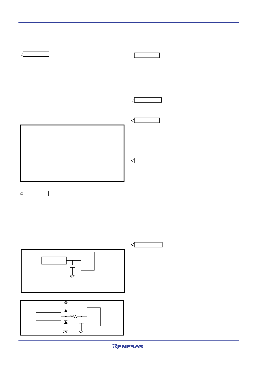
Fig. 73 Analog input external circuit example-1
A/D converter-2
Each analog input pin is equipped with a capacitor which is used
to compare the analog voltage. Accordingly, when the analog volt-
age is input from the circuit with high-impedance and, charge/
discharge noise is generated and the sufficient A/D accuracy may
not be obtained. Therefore, reduce the impedance or, connect a
capacitor (0.01
F to 1 F) to analog input pins (Figure 73).
When the overvoltage applied to the A/D conversion circuit may
occur, connect an external circuit in order to keep the voltage
within the rated range as shown the Figure 74. In addition, test
the application products sufficiently.
Sensor
AIN
Apply the voltage withiin the specifications
to an analog input pin.
Sensor
AIN
About 1k
18
19
Fig. 74 Analog input external circuit example-2
21
相关PDF资料 |
PDF描述 |
|---|---|
| M34519M6-XXXFP | 4-BIT, MROM, 6 MHz, MICROCONTROLLER, PDSO42 |
| M34553M8H-XXXFP | 4-BIT, MROM, 6 MHz, MICROCONTROLLER, PQFP48 |
| M34553M4-XXXFP | 4-BIT, MROM, 6 MHz, MICROCONTROLLER, PQFP48 |
| M34553G8HFP | 4-BIT, OTPROM, 6 MHz, MICROCONTROLLER, PQFP48 |
| M34553M4H-XXXFP | 4-BIT, MROM, 6 MHz, MICROCONTROLLER, PQFP48 |
相关代理商/技术参数 |
参数描述 |
|---|---|
| M34-52 | 制造商:GAMEWELL-FCI 制造商全称:GAMEWELL-FCI 功能描述:Three-Fold Fire Alarm Boxes and Transmitters |
| M34524EDFP | 制造商:RENESAS 制造商全称:Renesas Technology Corp 功能描述:SINGLE-CHIP 4-BIT CMOS MICROCOMPUTER |
| M34524M8-XXXFP | 制造商:RENESAS 制造商全称:Renesas Technology Corp 功能描述:SINGLE-CHIP 4-BIT CMOS MICROCOMPUTER |
| M34524MC-XXXFP | 制造商:RENESAS 制造商全称:Renesas Technology Corp 功能描述:4-BIT CISC SINGLE-CHIP MICROCOMPUTER 720 FAMILY / 4500 SERIES |
| M3452-C09K1 | 制造商:Bonitron 功能描述:OVERVOLTAGE BRAKING TRANSISTOR |
发布紧急采购,3分钟左右您将得到回复。