- 您现在的位置:买卖IC网 > PDF目录299435 > M50FLW080AN5G (STMICROELECTRONICS) 1M X 8 FLASH 3V PROM, 11 ns, PDSO40 PDF资料下载
参数资料
| 型号: | M50FLW080AN5G |
| 厂商: | STMICROELECTRONICS |
| 元件分类: | PROM |
| 英文描述: | 1M X 8 FLASH 3V PROM, 11 ns, PDSO40 |
| 封装: | 10 X 20 MM, ROHS COMPLIANT, PLASTIC, TSOP-40 |
| 文件页数: | 13/64页 |
| 文件大小: | 534K |
| 代理商: | M50FLW080AN5G |
第1页第2页第3页第4页第5页第6页第7页第8页第9页第10页第11页第12页当前第13页第14页第15页第16页第17页第18页第19页第20页第21页第22页第23页第24页第25页第26页第27页第28页第29页第30页第31页第32页第33页第34页第35页第36页第37页第38页第39页第40页第41页第42页第43页第44页第45页第46页第47页第48页第49页第50页第51页第52页第53页第54页第55页第56页第57页第58页第59页第60页第61页第62页第63页第64页
Bus operations
M50FLW080A, M50FLW080B
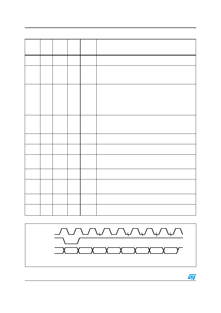
Figure 6.
FWH Bus Read waveforms
Table 6.
FWH Bus Read field definitions
Clock
Cycle
Number
Clock
Cycle
Count
Field
FWH0-
FWH3
Memory
I/O
Description
1
START
1101b
I
On the rising edge of CLK with FWH4 Low, the contents of FWH0-
FWH3 indicate the start of a FWH Read cycle.
2
1
IDSEL
XXXX
I
Indicates which FWH Flash Memory is selected. The value on
FWH0-FWH3 is compared to the IDSEL strapping on the FWH
Flash Memory pins to select which FWH Flash Memory is being
addressed.
3-9
7
ADDR
XXXX
I
A 28-bit address is transferred, with the most significant nibble
first. For the multi-byte read operation, the least significant bits
(MSIZE of them) are treated as Don't Care, and the read operation
is started with each of these bits reset to 0. Address lines A20-21
and A23-27 are treated as Don’t Care during a normal memory
array access, with A22=1, but are taken into account for a register
access, with A22=0. (See Table 15)
10
1
MSIZE
XXXX
I
This one clock cycle is driven by the host to determine the number
of Bytes that will be transferred. M50FLW080 supports: single
Byte transfer (0000b), 2-Byte transfer (0001b), 4-Byte transfer
(0010b), 16-Byte transfer (0100b) and 128-Byte transfer (0111b).
11
1
TAR
1111b
I
The host drives FWH0-FWH3 to 1111b to indicate a turnaround
cycle.
12
1
TAR
1111b
(float)
O
The FWH Flash Memory takes control of FWH0-FWH3 during this
cycle.
13-14
2
WSYNC 0101b
O
The FWH Flash Memory drives FWH0-FWH3 to 0101b (short
wait-sync) for two clock cycles, indicating that the data is not yet
available. Two wait-states are always included.
15
1
RSYNC
0000b
O
The FWH Flash Memory drives FWH0-FWH3 to 0000b, indicating
that data will be available during the next clock cycle.
16-17
M=2n
DATA
XXXX
O
Data transfer is two CLK cycles, starting with the least significant
nibble. If multi-Byte read operation is enabled, repeat cycle-16 and
cycle-17 n times, where n = 2MSIZE.
previous
+1
1
TAR
1111b
O
The FWH Flash Memory drives FWH0-FWH3 to 1111b to indicate
a turnaround cycle.
previous
+1
1TAR
1111b
(float)
N/A
The FWH Flash Memory floats its outputs, the host takes control
of FWH0-FWH3.
AI08433B
CLK
FWH4
FWH0-FWH3
Number of
clock cycles
START
IDSEL
ADDR
MSIZE
TAR
SYNC
DATA
TAR
117123
M
2
相关PDF资料 |
PDF描述 |
|---|---|
| M50FLW080BN5G | 1M X 8 FLASH 3V PROM, 11 ns, PDSO40 |
| M5218 | CAP .68UF 50V ELECT MVK BI SMD |
| M5278L12 | 12 V FIXED POSITIVE REGULATOR, PBCY3 |
| M54193P | TELEPHONE RINGER CKT, PDIP8 |
| M54HC4066F1 | QUAD 1-CHANNEL, SGL POLE SGL THROW SWITCH, CDIP14 |
相关代理商/技术参数 |
参数描述 |
|---|---|
| M50FLW080AN5P | 制造商:STMICROELECTRONICS 制造商全称:STMicroelectronics 功能描述:8 Mbit (13 x 64KByte Blocks + 3 x 16 x 4KByte Sectors), 3V Supply Firmware Hub / Low Pin Count Flash Memory |
| M50FLW080AN5T | 制造商:STMICROELECTRONICS 制造商全称:STMicroelectronics 功能描述:8 Mbit (13 x 64KByte Blocks + 3 x 16 x 4KByte Sectors), 3V Supply Firmware Hub / Low Pin Count Flash Memory |
| M50FLW080AN5TG | 功能描述:IC FLASH 8MBIT 33MHZ 40TSOP RoHS:是 类别:集成电路 (IC) >> 存储器 系列:- 标准包装:1,000 系列:- 格式 - 存储器:RAM 存储器类型:移动 SDRAM 存储容量:256M(8Mx32) 速度:133MHz 接口:并联 电源电压:1.7 V ~ 1.95 V 工作温度:-40°C ~ 85°C 封装/外壳:90-VFBGA 供应商设备封装:90-VFBGA(8x13) 包装:带卷 (TR) 其它名称:557-1327-2 |
| M50FLW080AN5TP | 制造商:STMICROELECTRONICS 制造商全称:STMicroelectronics 功能描述:8 Mbit (13 x 64KByte Blocks + 3 x 16 x 4KByte Sectors), 3V Supply Firmware Hub / Low Pin Count Flash Memory |
| M50FLW080ANB5 | 制造商:STMICROELECTRONICS 制造商全称:STMicroelectronics 功能描述:8 Mbit (13 x 64KByte Blocks + 3 x 16 x 4KByte Sectors), 3V Supply Firmware Hub / Low Pin Count Flash Memory |
发布紧急采购,3分钟左右您将得到回复。