- 您现在的位置:买卖IC网 > PDF目录299435 > M50FLW080AN5G (STMICROELECTRONICS) 1M X 8 FLASH 3V PROM, 11 ns, PDSO40 PDF资料下载
参数资料
| 型号: | M50FLW080AN5G |
| 厂商: | STMICROELECTRONICS |
| 元件分类: | PROM |
| 英文描述: | 1M X 8 FLASH 3V PROM, 11 ns, PDSO40 |
| 封装: | 10 X 20 MM, ROHS COMPLIANT, PLASTIC, TSOP-40 |
| 文件页数: | 18/64页 |
| 文件大小: | 534K |
| 代理商: | M50FLW080AN5G |
第1页第2页第3页第4页第5页第6页第7页第8页第9页第10页第11页第12页第13页第14页第15页第16页第17页当前第18页第19页第20页第21页第22页第23页第24页第25页第26页第27页第28页第29页第30页第31页第32页第33页第34页第35页第36页第37页第38页第39页第40页第41页第42页第43页第44页第45页第46页第47页第48页第49页第50页第51页第52页第53页第54页第55页第56页第57页第58页第59页第60页第61页第62页第63页第64页
M50FLW080A, M50FLW080B
Command interface
4
Command interface
All Bus Write operations to the device are interpreted by the Command Interface.
Commands consist of one or more sequential Bus Write operations. An internal
Program/Erase Controller handles all timings, and verifies the correct execution of the
Program and Erase commands. The Program/Erase Controller provides a Status Register
whose output may be read at any time to monitor the progress or the result of the operation.
The Command Interface reverts to the Read mode when power is first applied, or when
exiting from Reset. Command sequences must be followed exactly. Any invalid combination
of commands will be ignored. See Table 11 for the available Command Codes.
The following commands are the basic commands used to read from, write to, and configure
the device. The following text descriptions should be read in conjunction with Table 13.
4.1
Read Memory Array command
The Read Memory Array command returns the device to its Read mode, where it behaves
like a ROM or EPROM. One Bus Write cycle is required to issue the Read Memory Array
command and return the device to Read mode. Once the command is issued, the device
remains in Read mode until another command is issued. From Read mode, Bus Read
operations access the memory array.
If the Program/Erase Controller is executing a Program or Erase operation, the device will
not accept any Read Memory Array commands until the operation has completed.
For a multibyte read, in the FWH mode, the address, that was transmitted with the
command, will be automatically aligned, according to the MSIZE granularity. For example, if
MSIZE=7, regardless of any values that are provided for A6-A0, the first output will be from
the location for which A6-A0 are all ‘0’s.
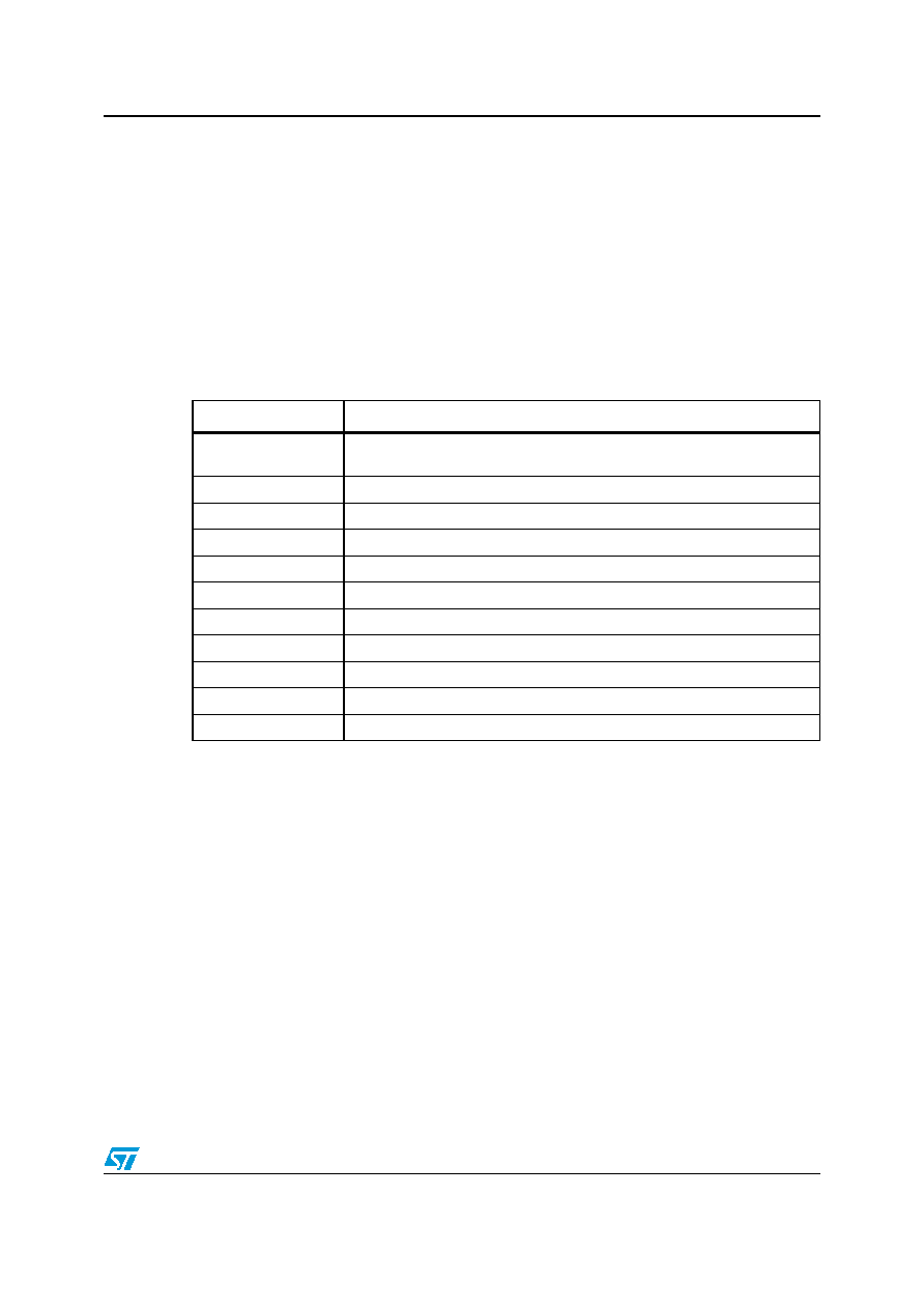
Table 11.
Command codes
Hexa-decimal
Command
10h
Alternative Program Setup, Double/Quadruple Byte Program Setup, Chip
Erase Confirm
20h
Block Erase Setup
32h
Sector Erase Setup
40h
Program, Double/Quadruple Byte Program Setup
50h
Clear Status Register
70h
Read Status Register
80h
Chip Erase Setup
90h
Read Electronic Signature
B0h
Program/Erase Suspend
D0h
Program/Erase Resume, Block Erase Confirm, Sector Erase Confirm
FFh
Read Memory Array
相关PDF资料 |
PDF描述 |
|---|---|
| M50FLW080BN5G | 1M X 8 FLASH 3V PROM, 11 ns, PDSO40 |
| M5218 | CAP .68UF 50V ELECT MVK BI SMD |
| M5278L12 | 12 V FIXED POSITIVE REGULATOR, PBCY3 |
| M54193P | TELEPHONE RINGER CKT, PDIP8 |
| M54HC4066F1 | QUAD 1-CHANNEL, SGL POLE SGL THROW SWITCH, CDIP14 |
相关代理商/技术参数 |
参数描述 |
|---|---|
| M50FLW080AN5P | 制造商:STMICROELECTRONICS 制造商全称:STMicroelectronics 功能描述:8 Mbit (13 x 64KByte Blocks + 3 x 16 x 4KByte Sectors), 3V Supply Firmware Hub / Low Pin Count Flash Memory |
| M50FLW080AN5T | 制造商:STMICROELECTRONICS 制造商全称:STMicroelectronics 功能描述:8 Mbit (13 x 64KByte Blocks + 3 x 16 x 4KByte Sectors), 3V Supply Firmware Hub / Low Pin Count Flash Memory |
| M50FLW080AN5TG | 功能描述:IC FLASH 8MBIT 33MHZ 40TSOP RoHS:是 类别:集成电路 (IC) >> 存储器 系列:- 标准包装:1,000 系列:- 格式 - 存储器:RAM 存储器类型:移动 SDRAM 存储容量:256M(8Mx32) 速度:133MHz 接口:并联 电源电压:1.7 V ~ 1.95 V 工作温度:-40°C ~ 85°C 封装/外壳:90-VFBGA 供应商设备封装:90-VFBGA(8x13) 包装:带卷 (TR) 其它名称:557-1327-2 |
| M50FLW080AN5TP | 制造商:STMICROELECTRONICS 制造商全称:STMicroelectronics 功能描述:8 Mbit (13 x 64KByte Blocks + 3 x 16 x 4KByte Sectors), 3V Supply Firmware Hub / Low Pin Count Flash Memory |
| M50FLW080ANB5 | 制造商:STMICROELECTRONICS 制造商全称:STMicroelectronics 功能描述:8 Mbit (13 x 64KByte Blocks + 3 x 16 x 4KByte Sectors), 3V Supply Firmware Hub / Low Pin Count Flash Memory |
发布紧急采购,3分钟左右您将得到回复。