参数资料
| 型号: | MAX3109ETJ+ |
| 厂商: | Maxim Integrated Products |
| 文件页数: | 8/66页 |
| 文件大小: | 0K |
| 描述: | SEMICONDUCTOR OTHER |
| 标准包装: | 60 |
| 系列: | * |
第1页第2页第3页第4页第5页第6页第7页当前第8页第9页第10页第11页第12页第13页第14页第15页第16页第17页第18页第19页第20页第21页第22页第23页第24页第25页第26页第27页第28页第29页第30页第31页第32页第33页第34页第35页第36页第37页第38页第39页第40页第41页第42页第43页第44页第45页第46页第47页第48页第49页第50页第51页第52页第53页第54页第55页第56页第57页第58页第59页第60页第61页第62页第63页第64页第65页第66页
Dual Serial UART with 128-Word FIFOs
MAX3109
16
Maxim Integrated
Detailed Description
The MAX3109 dual universal asynchronous receiver-
transmitter (UART) bridges an SPI/MICROWIREK or
I2C microprocessor bus to an asynchronous serial-data
communication link, such as RS-485, RS-232, or IrDA.
The MAX3109 is configured through 8-bit registers,
which are accessed through the SPI or I2C interface.
These registers are organized by related function as
shown in the Register Map section.
The host controller loads data into the Transmit Hold reg-
ister (THR) through the SPI or I2C interface. This data is
automatically pushed into the transmit FIFOs, formatted,
and sent out at TX_. The MAX3109 adds START, STOP,
and parity bits to the data before transmitting the data
out at the selected baud rate. The clock configuration
registers determine the baud rates, clock source selec-
tion, clock frequency prescaling, and fractional baud-
rate generator settings for each UART.
The MAX3109 receivers detect a START bit as a high-
to-low transition on RX_. An internal clock samples this
data at 16 times the baud rate. The received data is
automatically placed in the receive FIFOs and can then
be read out by the host controller through the Receiver
Hold register (RHR).
The device features two identical UARTs that are com-
pletely independent except for the input clock. Text in
this data sheet references individual UART operation,
unless otherwise noted.
The MAX3109’s register set is compatible with the MAX3107.
Refer to Application Note 4938: Differences Between
Maxim's Advanced UART Devices for information on how
to transfer firmware from the MAX3107 to the MAX3109.
Receive and Transmit FIFOs
Each UART’s receiver and transmitter has a 128-word-
deep FIFOs, reducing the number of intervals that the
host processor needs to dedicate for high-speed, high-
volume data transfer to and from the device. As the data
rates of the asynchronous RX_/TX_ interfaces increase
and get closer to those of the host controller’s SPI/I2C
data rates, UART management and flow-control can
make up a significant portion of the host’s activity. By
increasing FIFO size, the host is interrupted less often
and can use data block transfers to and from the FIFOs.
FIFO trigger levels can generate interrupts to the host
controller, signaling that programmed FIFO fill levels
have been reached. The transmitter and receiver trigger
levels are programmed through the FIFOTrgLvl register
with a resolution of eight FIFO locations. The receive
FIFO trigger signals to the host either that the receive
FIFO has a defined number of words waiting to be read
out in a block or that a known number of vacant FIFO
locations are available and ready to be filled. The trans-
mit FIFO trigger generates an interrupt when the transmit
FIFO fill level is above the programmed trigger level. The
host then knows to throttle data writing to the transmit
FIFO through THR.
The host can read out the number of words pres-
ent in each of the FIFOs through the TxFIFOLvl and
RxFIFOLvl registers.
MICROWIRE is a trademark of National Semiconductor Corp.
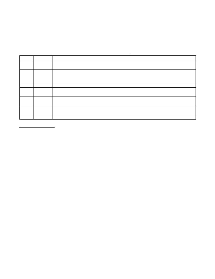
Pin Description (continued)
PIN
NAME
FUNCTION
27
XOUT
Crystal Output. When using an external crystal, connect one end of the crystal to XOUT and the other
end to XIN. When using an external clock source, leave XOUT unconnected.
28
GPIO6
General-Purpose Input/Output 6. GPIO6 is user-programmable as input or output (push-pull or open
drain) or an external event-driven interrupt source. GPIO6 has a weak pulldown resistor to DGND when
configured as an input.
29
AGND
Analog Ground
30
LDOEN
LDO Enable Input. Drive LDOEN high to enable the internal 1.8V LDO. Drive LDOEN low to disable the
internal LDO. Supply V18 with an external voltage source when LDOEN is low.
31
V18
Internal 1.8V LDO Output and 1.8V Power-Supply Input. Bypass V18 with a 1FF ceramic capacitor to
DGND.
32
VCC
Analog Power Supply. VCC powers the PLL and internal LDO. Bypass VCC with a 0.1FF ceramic
capacitor to AGND.
—
EP
Exposed Pad. Connect EP to AGND. Do not use EP as the main AGND connection.
相关PDF资料 |
PDF描述 |
|---|---|
| MAX310CPE | IC VIDEO MULTIPLEXER 8X1 16DIP |
| MAX3110EENI+G36 | IC UART SPI COMPAT 28-DIP |
| MAX3120CUA+ | IC TXRX INFRARED IRDA 8-UMAX |
| MAX3120EUA | IC TXRX 3V IRDA IR 3V 8-UMAX |
| MAX312ESE | IC SWITCH QUAD SPST 16SOIC |
相关代理商/技术参数 |
参数描述 |
|---|---|
| MAX3109ETJ+ | 功能描述:UART 接口集成电路 Dual Serial UART with 128-Word FIFOs RoHS:否 制造商:Texas Instruments 通道数量:2 数据速率:3 Mbps 电源电压-最大:3.6 V 电源电压-最小:2.7 V 电源电流:20 mA 最大工作温度:+ 85 C 最小工作温度:- 40 C 封装 / 箱体:LQFP-48 封装:Reel |
| MAX3109ETJ+T | 功能描述:UART 接口集成电路 Dual Serial UART with 128-Word FIFOs RoHS:否 制造商:Texas Instruments 通道数量:2 数据速率:3 Mbps 电源电压-最大:3.6 V 电源电压-最小:2.7 V 电源电流:20 mA 最大工作温度:+ 85 C 最小工作温度:- 40 C 封装 / 箱体:LQFP-48 封装:Reel |
| MAX310C/D | 功能描述:多路器开关 IC RoHS:否 制造商:Texas Instruments 通道数量:1 开关数量:4 开启电阻(最大值):7 Ohms 开启时间(最大值): 关闭时间(最大值): 传播延迟时间:0.25 ns 工作电源电压:2.3 V to 3.6 V 工作电源电流: 最大工作温度:+ 85 C 安装风格:SMD/SMT 封装 / 箱体:UQFN-16 |
| MAX310CPE | 功能描述:多路器开关 IC RoHS:否 制造商:Texas Instruments 通道数量:1 开关数量:4 开启电阻(最大值):7 Ohms 开启时间(最大值): 关闭时间(最大值): 传播延迟时间:0.25 ns 工作电源电压:2.3 V to 3.6 V 工作电源电流: 最大工作温度:+ 85 C 安装风格:SMD/SMT 封装 / 箱体:UQFN-16 |
| MAX310CPE+ | 功能描述:多路器开关 IC 8:1 Unbuffered RF Video MUX RoHS:否 制造商:Texas Instruments 通道数量:1 开关数量:4 开启电阻(最大值):7 Ohms 开启时间(最大值): 关闭时间(最大值): 传播延迟时间:0.25 ns 工作电源电压:2.3 V to 3.6 V 工作电源电流: 最大工作温度:+ 85 C 安装风格:SMD/SMT 封装 / 箱体:UQFN-16 |
发布紧急采购,3分钟左右您将得到回复。