- 您现在的位置:买卖IC网 > PDF目录13549 > MAX5073ETI+T (Maxim Integrated Products)IC REG BUCK BST ADJ 1A/2A 28TQFN PDF资料下载
参数资料
| 型号: | MAX5073ETI+T |
| 厂商: | Maxim Integrated Products |
| 文件页数: | 8/25页 |
| 文件大小: | 0K |
| 描述: | IC REG BUCK BST ADJ 1A/2A 28TQFN |
| 产品培训模块: | Lead (SnPb) Finish for COTS Obsolescence Mitigation Program |
| 标准包装: | 2,500 |
| 类型: | 降压(降压),升压(升压) |
| 输出类型: | 可调式 |
| 输出数: | 2 |
| 输出电压: | 0.8 V ~ 28 V |
| 输入电压: | 4.5 V ~ 23 V |
| PWM 型: | 电压模式 |
| 频率 - 开关: | 200kHz ~ 2.2MHz |
| 电流 - 输出: | 1A,2A |
| 同步整流器: | 无 |
| 工作温度: | -40°C ~ 85°C |
| 安装类型: | 表面贴装 |
| 封装/外壳: | 28-WFQFN 裸露焊盘 |
| 包装: | 带卷 (TR) |
| 供应商设备封装: | 28-TQFN-EP(5x5) |
�� �
�
�2.2MHz,� Dual-Output� Buck� or� Boost� Converter�
�with� Internal� Power� MOSFETs�
�Typical� Operating� Characteristics� (continued)�
�(V+� =� VL� =� 5.2V,� T� A� =� +25°C,� unless� otherwise� noted.)�
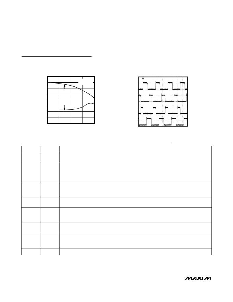
�3.00�
�OUTPUT� LOAD� CURRENT� LIMIT�
�vs.� TEMPERATURE�
�FOUR-PHASE� OPERATION�
�(SEE� FIGURE� 3)�
�MAX5073� toc22�
�2.75�
�2.50�
�2.25�
�2.00�
�1.75�
�1.50�
�OUTPUT1�
�OUTPUT2�
�V� IN� =� 5.5V�
�f� SW� =� 2.2MHz�
�SOURCE1�
�(MASTER)�
�0V�
�SOURCE2�
�(MASTER)�
�0V�
�SOURCE1�
�(SLAVE)�
�0V�
�1.25�
�SOURCE2�
�1.00�
�(SLAVE)�
�-40�
�-5�
�30�
�65�
�100�
�TEMPERATURE� (� °� C)�
�400ns/div�
�Pin� Description�
�PIN�
�1�
�2�
�3,� 4�
�5�
�6�
�7�
�8�
�9�
�NAME�
�CLKOUT�
�BST2/VDD2�
�DRAIN2�
�EN2�
�FB2�
�COMP2�
�SYNC�
�N.C.�
�FUNCTION�
�Clock� Output.� CLKOUT� is� 45°� phase-shifted� with� respect� to� converter� 2� (SOURCE2,� Figure� 3).� Connect�
�CLKOUT� (master)� to� the� SYNC� of� a� second� MAX5073� (slave)� for� a� four-phase� converter.�
�Buck� Converter� Operation—Bootstrap� Flying-Capacitor� Connection� for� Converter� 2.� Connect� BST2/VDD2�
�to� an� external� ceramic� capacitor� and� diode� according� to� the� standard� application� circuit� (Figure� 1).�
�Boost� Converter� Operation—Driver� Bypass� Capacitor� Connection.� Connect� a� low-ESR� 0.1μF� ceramic�
�capacitor� from� BST2/VDD2� to� PGND� (Figure� 8).�
�Connection� to� Converter� 2� Internal� MOSFET� Drain.� Buck� converter� operation—use� the� MOSFET� as� a�
�high-side� switch� and� connect� DRAIN2� to� the� input� supply.� Boost� converter� operation—use� the� MOSFET�
�as� a� low-side� switch� and� connect� DRAIN2� to� the� inductor� and� diode� junction� (Figure� 8).�
�Active-High� Enable� Input� for� Converter� 2.� Drive� EN2� low� to� shut� down� converter� 2,� drive� EN2� high� for� normal�
�operation.� Use� EN2� in� conjunction� with� EN1� for� supply� sequencing.� Connect� to� VL� for� always-on� operation.�
�Feedback� Input� for� Converter� 2.� Connect� FB2� to� a� resistive� divider� between� converter� 2’s� output� and� SGND�
�to� adjust� the� output� voltage.� To� set� the� output� voltage� below� 0.8V,� connect� FB2� to� a� resistive� voltage-divider�
�from� BYPASS� to� regulator� 2’s� output� (Figure� 5).� See� the� Setting� the� Output� Voltage� section.�
�Compensation� Connection� for� Converter� 2.� See� the� Compensation� section� to� compensate� converter� 2’s�
�control� loop.�
�External� Clock� Synchronization� Input.� Connect� SYNC� to� a� 400kHz� to� 4400kHz� clock� to� synchronize� the�
�switching� frequency� with� the� system� clock.� Each� converter� frequency� is� one� half� the� frequency� applied� to�
�SYNC.� Connect� SYNC� to� SGND� when� not� used.�
�No� Connection.� Not� internally� connected.�
�8�
�_______________________________________________________________________________________�
�相关PDF资料 |
PDF描述 |
|---|---|
| MAX16904SATB80/V+T | IC REG BUCK SYNC 8V 600MA 10TDFN |
| MAX16904SATB60/V+T | IC REG BUCK SYNC 6V 600MA 10TDFN |
| VI-J4T-EX-F4 | CONVERTER MOD DC/DC 6.5V 75W |
| MAX16904SATB51/V+T | IC REG BUCK SYNC 5.1V .6A 10TDFN |
| SCMS5D25-R50 | INDUCTOR SMD 0.50UH 4.9A100KHZ |
相关代理商/技术参数 |
参数描述 |
|---|---|
| MAX5073ETJ | 制造商:Maxim Integrated Products 功能描述:- Rail/Tube |
| MAX5074AAUP+T | 制造商:Maxim Integrated Products 功能描述: |
| MAX5074AUP | 功能描述:功率驱动器IC RoHS:否 制造商:Micrel 产品:MOSFET Gate Drivers 类型:Low Cost High or Low Side MOSFET Driver 上升时间: 下降时间: 电源电压-最大:30 V 电源电压-最小:2.75 V 电源电流: 最大功率耗散: 最大工作温度:+ 85 C 安装风格:SMD/SMT 封装 / 箱体:SOIC-8 封装:Tube |
| MAX5074AUP+ | 功能描述:功率驱动器IC for Iso IEEE 802.3af PD & Telecom Aps RoHS:否 制造商:Micrel 产品:MOSFET Gate Drivers 类型:Low Cost High or Low Side MOSFET Driver 上升时间: 下降时间: 电源电压-最大:30 V 电源电压-最小:2.75 V 电源电流: 最大功率耗散: 最大工作温度:+ 85 C 安装风格:SMD/SMT 封装 / 箱体:SOIC-8 封装:Tube |
| MAX5074AUP+T | 功能描述:功率驱动器IC for Iso IEEE 802.3af PD & Telecom Aps RoHS:否 制造商:Micrel 产品:MOSFET Gate Drivers 类型:Low Cost High or Low Side MOSFET Driver 上升时间: 下降时间: 电源电压-最大:30 V 电源电压-最小:2.75 V 电源电流: 最大功率耗散: 最大工作温度:+ 85 C 安装风格:SMD/SMT 封装 / 箱体:SOIC-8 封装:Tube |
发布紧急采购,3分钟左右您将得到回复。