- 您现在的位置:买卖IC网 > PDF目录80410 > MB90F543GPF-GE1 (FUJITSU LTD) 16-BIT, FLASH, 16 MHz, MICROCONTROLLER, PQFP100 PDF资料下载
参数资料
| 型号: | MB90F543GPF-GE1 |
| 厂商: | FUJITSU LTD |
| 元件分类: | 微控制器/微处理器 |
| 英文描述: | 16-BIT, FLASH, 16 MHz, MICROCONTROLLER, PQFP100 |
| 封装: | 14 X 20 MM, 3.35 MM HEIGHT, 0.65 MM PITCH, ROHS COMPLIANT, PLASTIC, QFP-100 |
| 文件页数: | 3/72页 |
| 文件大小: | 1798K |
| 代理商: | MB90F543GPF-GE1 |
第1页第2页当前第3页第4页第5页第6页第7页第8页第9页第10页第11页第12页第13页第14页第15页第16页第17页第18页第19页第20页第21页第22页第23页第24页第25页第26页第27页第28页第29页第30页第31页第32页第33页第34页第35页第36页第37页第38页第39页第40页第41页第42页第43页第44页第45页第46页第47页第48页第49页第50页第51页第52页第53页第54页第55页第56页第57页第58页第59页第60页第61页第62页第63页第64页第65页第66页第67页第68页第69页第70页第71页第72页
MB90540G/545G Series
DS07-13703-7E
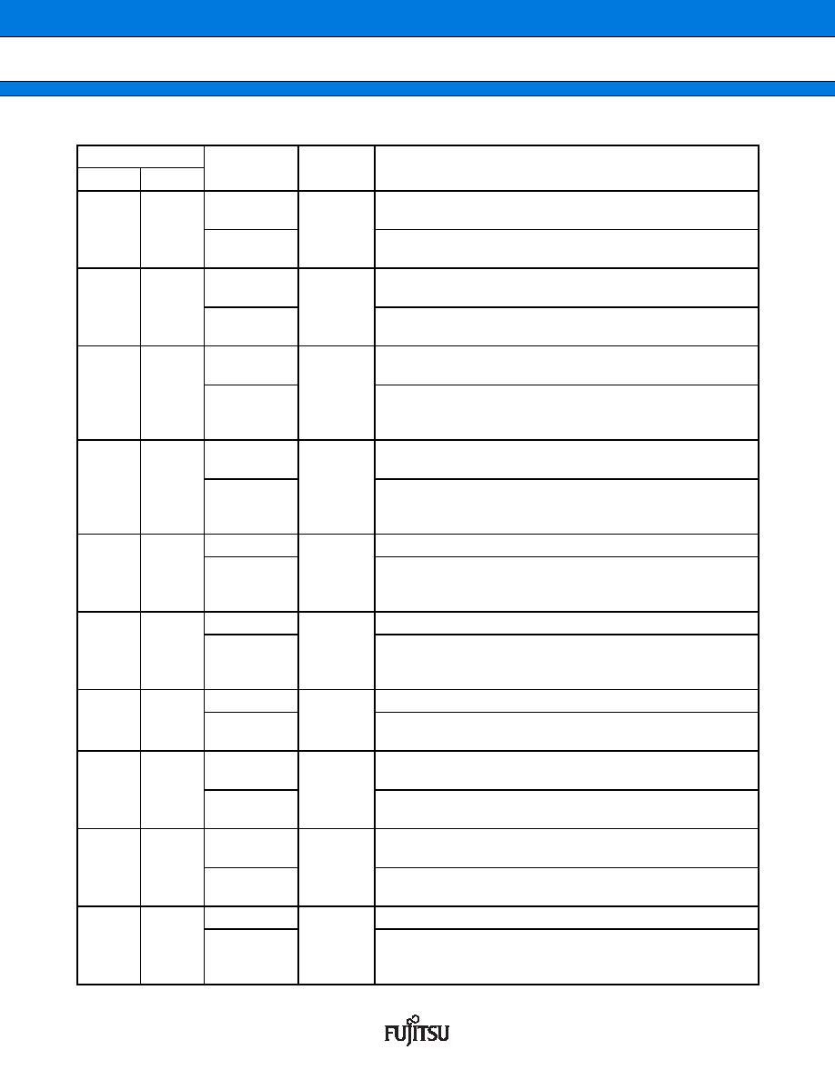
11
(Continued)
Pin No.
Pin name
Circuit
type
Function
LQFP*2
QFP*1
20
22
P44
G
General I/O port. This function is enabled when UART1
disables the clock output.
SCK1
Serial clock pulse I/O pin for UART1. This function is
enabled when UART1 enables the serial clock output.
22
24
P45
G
General I/O port. This function is enabled when UART1
disables the serial data output.
SOT1
Serial data output pin for UART1. This function is enabled when
UART1 enables the serial data output.
23
25
P46
G
General I/O port. This function is enabled when the Extended
I/O serial interface disables the serial data output.
SOT2
Serial data output pin for the Extended I/O serial interface. This
function is enabled when the Extended I/O serial interface en-
ables the serial data output.
24
26
P47
G
General I/O port. This function is enabled when the Extended
I/O serial interface disables the clock output.
SCK2
Serial clock pulse I/O pin for the Extended I/O serial interface .
This function is enabled when the Extended I/O serial interface
enables the Serial clock output.
26
28
P50
D
General I/O port. This function is always enabled.
SIN2
Serial data input pin for the Extended I/O serial interface . Set
the corresponding Port Direction Register to input if this func-
tion is used.
27 to 30
29 to 32
P51 to P54
D
General I/O port. This function is always enabled.
INT4 to INT7
External interrupt request input pins for INT4 to INT7. Set the
corresponding Port Direction Register to input if this function is
used.
31
33
P55
D
General I/O port. This function is always enabled.
ADTG
Trigger input pin for the A/D converter. Set the corresponding
Port Direction Register to input if this function is used.
36 to 39
38 to 41
P60 to P63
E
General I/O port. This function is enabled when the analog
input enable register specifies a port.
AN0 to AN3
Analog input pins for the 8/10-bit A/D converter. This function is
enabled when the analog input enable register specifies A/D.
41 to 44
43 to 46
P64 to P67
E
General I/O port. The function is enabled when the analog
input enable register specifies a port.
AN4 to AN7
Analog input pins for the 8/10-bit A/D converter. This function is
enabled when the analog input enable register specifies A/D.
45
47
P56
D
General I/O port. This function is always enabled.
TIN0
Event input pin for the 16-bit reload timers 0. Set the
corresponding Port Direction Register to input if this function is
used.
相关PDF资料 |
PDF描述 |
|---|---|
| MC9S12XF384J0CLMR | MICROCONTROLLER, PQFP112 |
| MPC8555ECVTAJE | RISC PROCESSOR, PBGA783 |
| MPC8360EVVAGDHA | 32-BIT, 400 MHz, RISC PROCESSOR, PBGA740 |
| MB95F263HP-G-SH-SNE2 | 8-BIT, FLASH, MICROCONTROLLER, PDIP24 |
| MB96F379RWAPMC1-GSE2 | 16-BIT, FLASH, 80 MHz, MICROCONTROLLER, PQFP144 |
相关代理商/技术参数 |
参数描述 |
|---|---|
| MB90F543GPFR-GE1 | 制造商:FUJITSU 功能描述: |
| MB90F543GSPFR-GE1 | 制造商:FUJITSU 功能描述: |
| MB90F543GSPMCR-GE1 | 制造商:FUJITSU 功能描述: |
| MB90F543PFR-GE1 | 制造商:FUJITSU 功能描述: |
| MB90F546GPFR-GE1 | 制造商:FUJITSU 功能描述: |
发布紧急采购,3分钟左右您将得到回复。