- 您现在的位置:买卖IC网 > PDF目录80410 > MB90F543GPF-GE1 (FUJITSU LTD) 16-BIT, FLASH, 16 MHz, MICROCONTROLLER, PQFP100 PDF资料下载
参数资料
| 型号: | MB90F543GPF-GE1 |
| 厂商: | FUJITSU LTD |
| 元件分类: | 微控制器/微处理器 |
| 英文描述: | 16-BIT, FLASH, 16 MHz, MICROCONTROLLER, PQFP100 |
| 封装: | 14 X 20 MM, 3.35 MM HEIGHT, 0.65 MM PITCH, ROHS COMPLIANT, PLASTIC, QFP-100 |
| 文件页数: | 41/72页 |
| 文件大小: | 1798K |
| 代理商: | MB90F543GPF-GE1 |
第1页第2页第3页第4页第5页第6页第7页第8页第9页第10页第11页第12页第13页第14页第15页第16页第17页第18页第19页第20页第21页第22页第23页第24页第25页第26页第27页第28页第29页第30页第31页第32页第33页第34页第35页第36页第37页第38页第39页第40页当前第41页第42页第43页第44页第45页第46页第47页第48页第49页第50页第51页第52页第53页第54页第55页第56页第57页第58页第59页第60页第61页第62页第63页第64页第65页第66页第67页第68页第69页第70页第71页第72页
MB90540G/545G Series
46
DS07-13703-7E
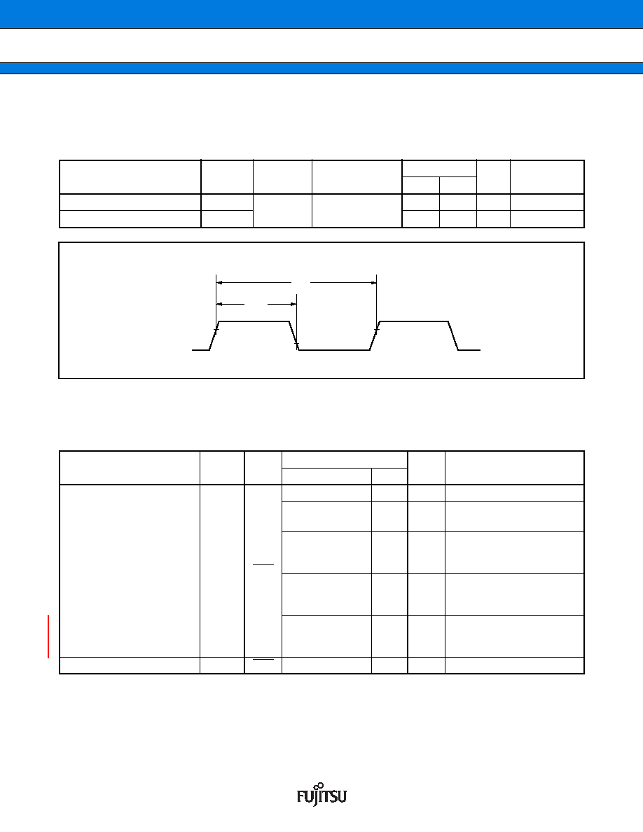
(2) Clock Output Timing
(MB90543G(S)/547G(S)/548G(S)/F548GL(S): VCC
= 3.5 V to 5.5 V, VSS = AVSS = 0.0 V, TA = 40 °C to +105 °C)
(Other than MB90543G(S)/547G(S)/548G(S)/F548GL(S):
VCC
= 5.0 V ± 10%, VSS = AVSS = 0.0 V, TA = 40 °C to +105 °C)
(3) Reset and Hardware Standby Input Timing
(MB90543G(S)/547G(S)/548G(S)/F548GL(S): VCC
= 3.5 V to 5.5 V, VSS = AVSS = 0.0 V, TA = 40 °C to +105 °C)
(Other than MB90543G(S)/547G(S)/548G(S)/F548GL(S):
VCC
= 5.0 V ± 10%, VSS = AVSS = 0.0 V, TA = 40 °C to +105 °C)
Note : “tcp” represents one cycle time of the machine clock.
Oscillation time of oscillator is time that amplitude reached the 90
%. In the crystal oscillator, the oscillation
time is between several ms to tens of ms. In ceramic oscillator, the oscillation time is between handreds of
s to several ms. In the external clock, the oscillation time is 0 ns.
Any reset can not fully initialize the Flash Memory if it is performing the automatic algorithm.
Parameter
Symbol
Pin name
Condition
Value
Units
Remarks
Min
Max
Cycle time
tCYC
CLK
VCC
= 5 V ± 10%
62.5
ns
CLK
↑ → CLK↓
tCHCL
20
ns
Parameter
Symbol
Pin
name
Value
Units
Remarks
Min
Max
Reset input time
tRSTL
RST
4 tCP
ns
Under normal operation
Oscillation time of
oscillator
+ 4 tCP
ms
In stop mode
100
s
In pseudo timer mode
(MB90543G (S) /547G (S) /
548G (S) )
4 tCP
ns
In pseudo timer mode
(Other than MB90543G (S) /
547G (S) /548G (S) )
2 tLCP
s
In sub-clock mode,
sub-sleep mode,
timer mode
Hardware standby input time
tHSTL
HST
4 tCP
ns
Under normal operation
CLK
tCYC
2.4 V
0.8 V
tCHCL
相关PDF资料 |
PDF描述 |
|---|---|
| MC9S12XF384J0CLMR | MICROCONTROLLER, PQFP112 |
| MPC8555ECVTAJE | RISC PROCESSOR, PBGA783 |
| MPC8360EVVAGDHA | 32-BIT, 400 MHz, RISC PROCESSOR, PBGA740 |
| MB95F263HP-G-SH-SNE2 | 8-BIT, FLASH, MICROCONTROLLER, PDIP24 |
| MB96F379RWAPMC1-GSE2 | 16-BIT, FLASH, 80 MHz, MICROCONTROLLER, PQFP144 |
相关代理商/技术参数 |
参数描述 |
|---|---|
| MB90F543GPFR-GE1 | 制造商:FUJITSU 功能描述: |
| MB90F543GSPFR-GE1 | 制造商:FUJITSU 功能描述: |
| MB90F543GSPMCR-GE1 | 制造商:FUJITSU 功能描述: |
| MB90F543PFR-GE1 | 制造商:FUJITSU 功能描述: |
| MB90F546GPFR-GE1 | 制造商:FUJITSU 功能描述: |
发布紧急采购,3分钟左右您将得到回复。