- 您现在的位置:买卖IC网 > PDF目录80410 > MB90F543GPF-GE1 (FUJITSU LTD) 16-BIT, FLASH, 16 MHz, MICROCONTROLLER, PQFP100 PDF资料下载
参数资料
| 型号: | MB90F543GPF-GE1 |
| 厂商: | FUJITSU LTD |
| 元件分类: | 微控制器/微处理器 |
| 英文描述: | 16-BIT, FLASH, 16 MHz, MICROCONTROLLER, PQFP100 |
| 封装: | 14 X 20 MM, 3.35 MM HEIGHT, 0.65 MM PITCH, ROHS COMPLIANT, PLASTIC, QFP-100 |
| 文件页数: | 72/72页 |
| 文件大小: | 1798K |
| 代理商: | MB90F543GPF-GE1 |
第1页第2页第3页第4页第5页第6页第7页第8页第9页第10页第11页第12页第13页第14页第15页第16页第17页第18页第19页第20页第21页第22页第23页第24页第25页第26页第27页第28页第29页第30页第31页第32页第33页第34页第35页第36页第37页第38页第39页第40页第41页第42页第43页第44页第45页第46页第47页第48页第49页第50页第51页第52页第53页第54页第55页第56页第57页第58页第59页第60页第61页第62页第63页第64页第65页第66页第67页第68页第69页第70页第71页当前第72页
MB90540G/545G Series
DS07-13703-7E
9
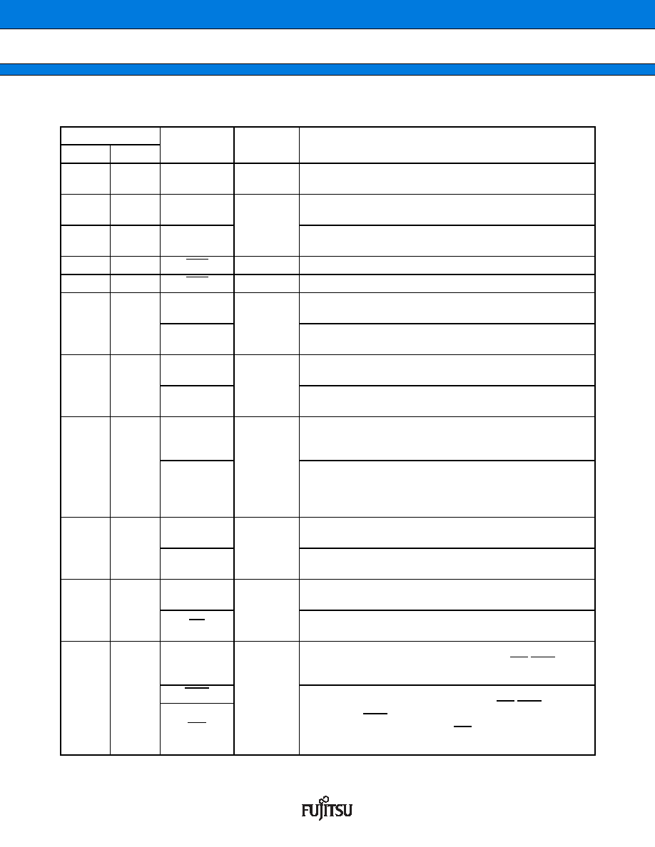
■ PIN DESCRIPTION
(Continued)
Pin No.
Pin name
Circuit type
Function
LQFP*2
QFP*1
80
81
82
83
X0
X1
A
(Oscillation)
High speed crystal oscillator input pins
78
80
X0A
A
(Oscillation)
Low speed crystal oscillator input pins. For the one clock sys-
tem parts, perfom external pull-down processing.
77
79
X1A
Low speed crystal oscillator input pins. For the one clock sys-
tem parts, leave it open.
75
77
RST
B
External reset request input pin
50
52
HST
C
Hardware standby input pin
83 to 90
85 to 92
P00 to P07
I
General I/O port with programmable pullup. This function is
enabled in the single-chip mode.
AD00 to AD07
I/O pins for 8 lower bits of the external address/data bus. This
function is enabled when the external bus is enabled.
91 to 98 93 to 100
P10 to P17
I
General I/O port with programmable pullup. This function is
enabled in the single-chip mode.
AD08 to AD15
I/O pins for 8 higher bits of the external address/data bus. This
function is enabled when the external bus is enabled.
99 to 6
1 to 8
P20 to P27
I
General I/O port with programmable pullup. In external bus
mode, this function is valid when the corresponding bits in the
external address output control resister (HACR) are set to “1”.
A16 to A23
8-bit I/O pins for A16 to A23 at the external address/data bus.
In external bus mode, this function is valid when the corre-
sponding bits in the external address output control resister
(HACR) are set to “0”.
79
P30
I
General I/O port with programmable pullup. This function is
enabled in the single-chip mode.
ALE
Address latch enable output pin. This function is enabled
when the external bus is enabled.
810
P31
I
General I/O port with programmable pullup. This function is
enabled in the single-chip mode.
RD
Read strobe output pin for the data bus. This function is en-
abled when the external bus is enabled.
10
12
P32
I
General I/O port with programmable pullup. This function is
enabled in the single-chip mode or when the WR/WRL pin out-
put is disabled.
WRL
Write strobe output pin for the data bus. This function is en-
abled when both the external bus and the WR/WRL pin output
are enabled. WRL is write-strobe output pin for the lower 8 bits
of the data bus in 16-bit access. WR is write-strobe output pin
for the 8 bits of the data bus in 8-bit access.
WR
相关PDF资料 |
PDF描述 |
|---|---|
| MC9S12XF384J0CLMR | MICROCONTROLLER, PQFP112 |
| MPC8555ECVTAJE | RISC PROCESSOR, PBGA783 |
| MPC8360EVVAGDHA | 32-BIT, 400 MHz, RISC PROCESSOR, PBGA740 |
| MB95F263HP-G-SH-SNE2 | 8-BIT, FLASH, MICROCONTROLLER, PDIP24 |
| MB96F379RWAPMC1-GSE2 | 16-BIT, FLASH, 80 MHz, MICROCONTROLLER, PQFP144 |
相关代理商/技术参数 |
参数描述 |
|---|---|
| MB90F543GPFR-GE1 | 制造商:FUJITSU 功能描述: |
| MB90F543GSPFR-GE1 | 制造商:FUJITSU 功能描述: |
| MB90F543GSPMCR-GE1 | 制造商:FUJITSU 功能描述: |
| MB90F543PFR-GE1 | 制造商:FUJITSU 功能描述: |
| MB90F546GPFR-GE1 | 制造商:FUJITSU 功能描述: |
发布紧急采购,3分钟左右您将得到回复。