- 您现在的位置:买卖IC网 > PDF目录132984 > MB9AF311MPMC 32-BIT, FLASH, 40 MHz, RISC MICROCONTROLLER, PQFP80 PDF资料下载
参数资料
| 型号: | MB9AF311MPMC |
| 元件分类: | 微控制器/微处理器 |
| 英文描述: | 32-BIT, FLASH, 40 MHz, RISC MICROCONTROLLER, PQFP80 |
| 封装: | 0.50 MM PITCH, PLASTIC, LQFP-80 |
| 文件页数: | 9/114页 |
| 文件大小: | 1357K |
| 代理商: | MB9AF311MPMC |
第1页第2页第3页第4页第5页第6页第7页第8页当前第9页第10页第11页第12页第13页第14页第15页第16页第17页第18页第19页第20页第21页第22页第23页第24页第25页第26页第27页第28页第29页第30页第31页第32页第33页第34页第35页第36页第37页第38页第39页第40页第41页第42页第43页第44页第45页第46页第47页第48页第49页第50页第51页第52页第53页第54页第55页第56页第57页第58页第59页第60页第61页第62页第63页第64页第65页第66页第67页第68页第69页第70页第71页第72页第73页第74页第75页第76页第77页第78页第79页第80页第81页第82页第83页第84页第85页第86页第87页第88页第89页第90页第91页第92页第93页第94页第95页第96页第97页第98页第99页第100页第101页第102页第103页第104页第105页第106页第107页第108页第109页第110页第111页第112页第113页第114页
ATmega48PA/88PA/168PA [DATASHEET]
9223F–AVR–04/14
106
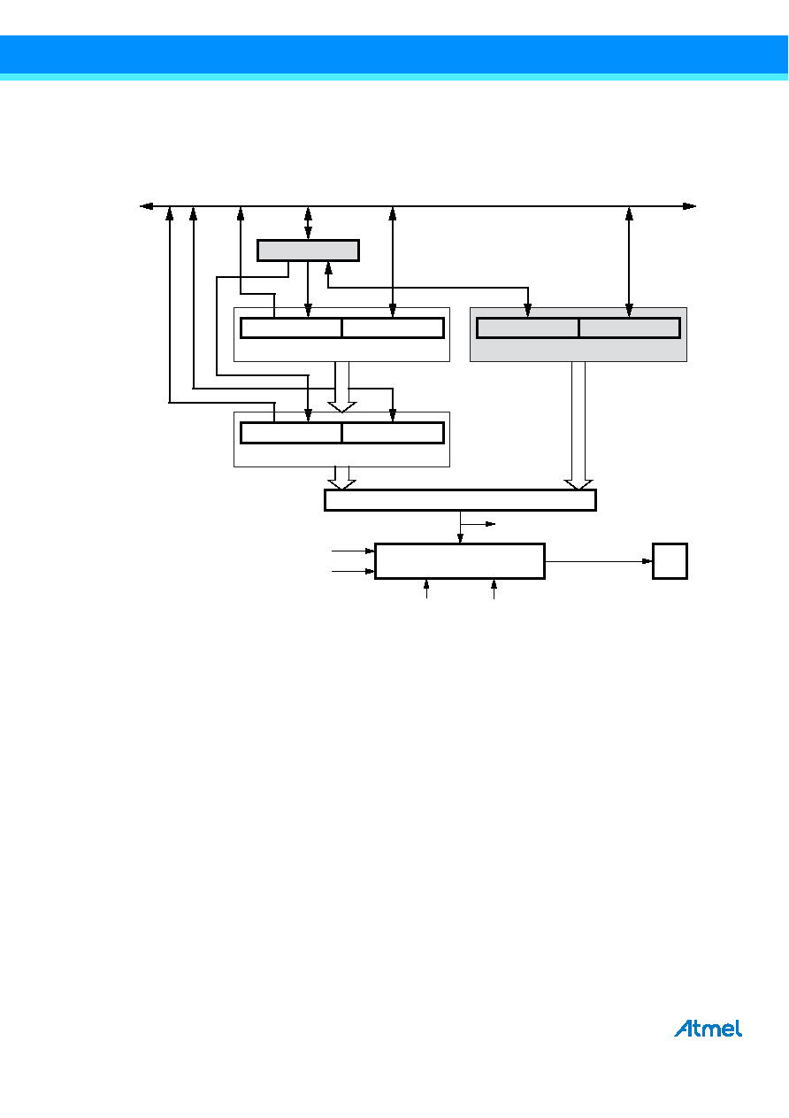
Figure 16-4 shows a block diagram of the output compare unit. The small “n” in the register and bit names indicates the
device number (n = 1 for Timer/Counter 1), and the “x” indicates output compare unit (A/B). The elements of the block
diagram that are not directly a part of the output compare unit are gray shaded.
Figure 16-4. Output Compare Unit, Block Diagram
The OCR1x register is double buffered when using any of the twelve pulse width modulation (PWM) modes. For the normal
and clear timer on compare (CTC) modes of operation, the double buffering is disabled. The double buffering synchronizes
the update of the OCR1x compare register to either TOP or BOTTOM of the counting sequence. The synchronization
prevents the occurrence of odd-length, non-symmetrical PWM pulses, thereby making the output glitch-free.
The OCR1x register access may seem complex, but this is not case. When the double buffering is enabled, the CPU has
access to the OCR1x buffer register, and if double buffering is disabled the CPU will access the OCR1x directly. The content
of the OCR1x (buffer or compare) register is only changed by a write operation (the Timer/Counter does not update this
register automatically as the TCNT1 and ICR1 register). Therefore OCR1x is not read via the high byte temporary register
(TEMP). However, it is a good practice to read the low byte first as when accessing other 16-bit registers. Writing the OCR1x
registers must be done via the TEMP register since the compare of all 16 bits is done continuously. The high byte (OCR1xH)
has to be written first. When the high byte I/O location is written by the CPU, the TEMP register will be updated by the value
written. Then when the low byte (OCR1xL) is written to the lower eight bits, the high byte will be copied into the upper 8-bits
of either the OCR1x buffer or OCR1x compare register in the same system clock cycle.
For more information of how to access the 16-bit registers refer to Section 16.3 “Accessing 16-bit Registers” on page 100.
16.7.1 Force Output Compare
In non-PWM waveform generation modes, the match output of the comparator can be forced by writing a one to the force
output compare (FOC1x) bit. Forcing compare match will not set the OCF1x Flag or reload/clear the timer, but the OC1x pin
will be updated as if a real compare match had occurred (the COM11:0 bits settings define whether the OC1x pin is set,
cleared or toggled).
OCRnxL Buf. (8-bit)
OCRnxH Buf. (8-bit)
OCRnx Buffer (16-bit Register)
TEMP (8-bit)
OCRnxL (8-bit)
OCFnx (Int. Req.)
OCRnxH (8-bit)
OCRnx (16-bit Register)
= (16-bitComparator)
WGMn3:0
COMnx1:0
Waveform Generator
TCNTnL (8-bit)
TCNTnH (8-bit)
TCNTn (16-bit Counter)
DATA BUS (8-bit)
OCnx
TOP
BOTTOM
相关PDF资料 |
PDF描述 |
|---|---|
| MSP430G2152IRSA16 | 16-BIT, FLASH, 16 MHz, RISC MICROCONTROLLER, PQCC16 |
| M37704E2EFP | 16-BIT, OTPROM, 16 MHz, MICROCONTROLLER, PQFP80 |
| MSM65544-JS | 8-BIT, MROM, 10 MHz, MICROCONTROLLER, PQCC68 |
| MSM65516SS | 8-BIT, MROM, 10 MHz, MICROCONTROLLER, PDIP64 |
| MSM65P512JS | 8-BIT, OTPROM, 10 MHz, MICROCONTROLLER, PQCC44 |
相关代理商/技术参数 |
参数描述 |
|---|---|
| MB9AF312KPMC1-G-JNE2 | 功能描述:ARM? Cortex?-M3 FM3 MB9A310K Microcontroller IC 32-Bit 40MHz 160KB (160K x 8) FLASH 52-LQFP (10x10) 制造商:cypress semiconductor corp 系列:FM3 MB9A310K 包装:托盘 零件状态:有效 核心处理器:ARM? Cortex?-M3 核心尺寸:32-位 速度:40MHz 连接性:CSIO,I2C,LIN,UART/USART,USB 外设:DMA,LVD,POR,PWM,WDT I/O 数:36 程序存储容量:160KB(160K x 8) 程序存储器类型:闪存 EEPROM 容量:- RAM 容量:16K x 8 电压 - 电源(Vcc/Vdd):2.7 V ~ 5.5 V 数据转换器:A/D 8x12b 振荡器类型:内部 工作温度:-40°C ~ 105°C(TA) 封装/外壳:52-LQFP 供应商器件封装:52-LQFP(10x10) 标准包装:160 |
| MB9AF312KPMC-ES-E1 | 制造商:FUJITSU 功能描述: |
| MB9AF312KPMC-G-JNE1 | 制造商:FUJITSU 功能描述: |
| MB9AF312KPMC-G-JNE2 | 功能描述:ARM? Cortex?-M3 FM3 MB9A310K Microcontroller IC 32-Bit 40MHz 160KB (160K x 8) FLASH 48-LQFP (7x7) 制造商:cypress semiconductor corp 系列:FM3 MB9A310K 包装:托盘 零件状态:有效 核心处理器:ARM? Cortex?-M3 核心尺寸:32-位 速度:40MHz 连接性:CSIO,I2C,LIN,UART/USART,USB 外设:DMA,LVD,POR,PWM,WDT I/O 数:36 程序存储容量:160KB(160K x 8) 程序存储器类型:闪存 EEPROM 容量:- RAM 容量:16K x 8 电压 - 电源(Vcc/Vdd):2.7 V ~ 5.5 V 数据转换器:A/D 8x12b 振荡器类型:内部 工作温度:-40°C ~ 105°C(TA) 封装/外壳:48-LQFP 供应商器件封装:48-LQFP(7x7) 标准包装:250 |
| MB9AF312KQN-ES-AWE2 | 制造商:FUJITSU 功能描述: |
发布紧急采购,3分钟左右您将得到回复。