- 您现在的位置:买卖IC网 > PDF目录371016 > MC145572 (Motorola, Inc.) ISDN U-Interface Transceiver(ISDN U接口收发器) PDF资料下载
参数资料
| 型号: | MC145572 |
| 厂商: | Motorola, Inc. |
| 英文描述: | ISDN U-Interface Transceiver(ISDN U接口收发器) |
| 中文描述: | 综合业务数字网U型接口收发器(综合业务数字网ü接口收发器) |
| 文件页数: | 94/264页 |
| 文件大小: | 2832K |
| 代理商: | MC145572 |
第1页第2页第3页第4页第5页第6页第7页第8页第9页第10页第11页第12页第13页第14页第15页第16页第17页第18页第19页第20页第21页第22页第23页第24页第25页第26页第27页第28页第29页第30页第31页第32页第33页第34页第35页第36页第37页第38页第39页第40页第41页第42页第43页第44页第45页第46页第47页第48页第49页第50页第51页第52页第53页第54页第55页第56页第57页第58页第59页第60页第61页第62页第63页第64页第65页第66页第67页第68页第69页第70页第71页第72页第73页第74页第75页第76页第77页第78页第79页第80页第81页第82页第83页第84页第85页第86页第87页第88页第89页第90页第91页第92页第93页当前第94页第95页第96页第97页第98页第99页第100页第101页第102页第103页第104页第105页第106页第107页第108页第109页第110页第111页第112页第113页第114页第115页第116页第117页第118页第119页第120页第121页第122页第123页第124页第125页第126页第127页第128页第129页第130页第131页第132页第133页第134页第135页第136页第137页第138页第139页第140页第141页第142页第143页第144页第145页第146页第147页第148页第149页第150页第151页第152页第153页第154页第155页第156页第157页第158页第159页第160页第161页第162页第163页第164页第165页第166页第167页第168页第169页第170页第171页第172页第173页第174页第175页第176页第177页第178页第179页第180页第181页第182页第183页第184页第185页第186页第187页第188页第189页第190页第191页第192页第193页第194页第195页第196页第197页第198页第199页第200页第201页第202页第203页第204页第205页第206页第207页第208页第209页第210页第211页第212页第213页第214页第215页第216页第217页第218页第219页第220页第221页第222页第223页第224页第225页第226页第227页第228页第229页第230页第231页第232页第233页第234页第235页第236页第237页第238页第239页第240页第241页第242页第243页第244页第245页第246页第247页第248页第249页第250页第251页第252页第253页第254页第255页第256页第257页第258页第259页第260页第261页第262页第263页第264页
MC145572
5–22
MOTOROLA
The MC145572 has a timeslot assigner that can be used when configured for MCU mode. The timeslot
assigner is enabled when one or more of OR6(b7, b6, or b5) are set to a 1. The starting timeslot(s)
are programmed into Overlay registers OR0 – OR5. The B1, B2, and D channels are each indepen-
dently programmable for both transmit and receive directions.
Timeslots are each two DCL clocks wide. Timeslot numbering starts from timeslot 0. Timeslot 0
occurs during the first two DCL clocks following FSX or FSR. DCL clocks are numbered starting from
0. Clock number 0 is the first DCL clock after the frame sync pulse FSX or FSR. Since FSX and FSR
can occur at different times, DCL clocks are counted referenced to either FSX or FSR depending on
which data direction is being configured. The timeslot number is calculated by counting the DCL
clocks after the appropriate frame sync where it is desired to place the start of the B or D channel
timeslot. This DCL count is divided by two and the resulting value is written to the appropriate timeslot
register.
The D channel data is always two contiguous DCL clocks or one timeslot in duration. B channel data
is always eight contiguous DCL clocks or four timeslots in duration. B channel timeslots may be pro-
grammed to start in any timeslot, though in normal applications, B channel timeslots are programmed
to start on every fourth timeslot or eighth DCL clock. Data is transferred between MC145572 and the
IDL2 interface only during B1, B2, or D channel timeslots that are enabled. When a B or D channel
timeslot is disabled, data appearing at the Din pin is ignored and the Dout pin is high impedance.
Table 5–5 details the timeslot assigner registers in the overlay register set. See Figures 5–27 and
5–28 for timeslot format examples.
The register programming for Figure 5–27 is as follows:
OR0 = $04
OR1 = $0B
OR2 = $01
OR3 = $00
OR4 = $08
OR5 = $0D
OR6 = $E0
OR7 = $20
OR8 = $08
The register programming for Figure 5–28 is as follows:
OR0 = $00
OR2 = $0D
OR3 = $04
OR5 = $01
OR6 = $50
OR7 = $20
OR8 = $08
The register programming for Figure 5–29 is as follows:
OR0 = $00
OR1 = $0B
OR2 = $08
OR3 = $00
OR4 = $0B
OR5 = $08
OR6 = $E0
OR7 = $00
OR8 = $09
Enabling the timeslot assigner overrides all other IDL2 frame formats with the exception of GCI 2B+D.
In GCI 2B+D data format, OR5 bits 2:0 are used to select the active GCI channel.
When the D channel port is enabled, the corresponding D channel timeslot is not enabled on the IDL2
interface. Instead, the D channel data is transferred over the D channel port referenced to FSR as
programmed in Overlay registers OR2 or OR5. This is also true when IDL2 GCI 2B+D mode has been
enabled. The Dout pin of the IDL2 interface is high impedance and data at Din is ignored. Figure 5–29
gives an example of D channel port operation when the timeslot assigner is enabled.
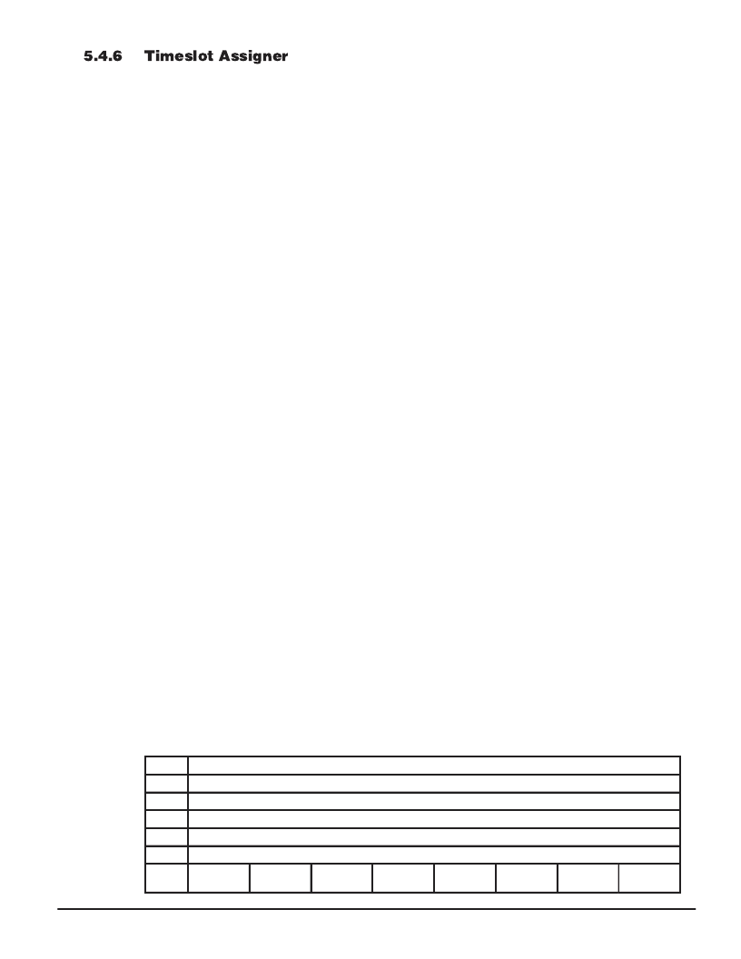
Table 5–5. Timeslot Assigner Registers
OR0
Dout B1 Channel Timeslot Bits (7:0)
Dout B2 Channel Timeslot Bits (7:0)
Dout D Channel Timeslot Bits (7:0)
Din B1 Channel Timeslot Bits (7:0)
Din B2 Channel Timeslot Bits (7:0)
Din D Channel Timeslot Bits (7:0) and GCI Slot (2:0)
TSA
D Enable
M4 – BR0
OR1
OR2
OR3
OR4
OR5
OR6
TSA
B1 Enable
TSA
B2 Enable
GCI Select
GCI Mode
Enable
Reserved
Reserved
Reserved
相关PDF资料 |
PDF描述 |
|---|---|
| MC145576 | ISDN NT1(ISDN 网络终端) |
| MC14557BCL | 1-to-64 Bit Variable Length Shift Register |
| MC14557BFEL | 1-to-64 Bit Variable Length Shift Register |
| MC14557BDWR2 | RJZ Series - Econoline Unregulated DC-DC Converters; Input Voltage (Vdc): 09V; Output Voltage (Vdc): 12V; Power: 2W; 2W Single and Dual Outputs in DIP 14; 3kVDC and 4kVDC Isolation; Optional Continuous Short Circuit Protected; Custom Solutions Available; UL94V-0 Package Material; Efficiency up to 85% |
| MC14557 | 1-to-64 Bit Variable Length Shift Register |
相关代理商/技术参数 |
参数描述 |
|---|---|
| MC145572AAC | 功能描述:IC TRANSCEIVER ISDN 44-LQFP RoHS:是 类别:集成电路 (IC) >> 接口 - 驱动器,接收器,收发器 系列:- 标准包装:1,000 系列:- 类型:收发器 驱动器/接收器数:2/2 规程:RS232 电源电压:3 V ~ 5.5 V 安装类型:表面贴装 封装/外壳:16-SOIC(0.295",7.50mm 宽) 供应商设备封装:16-SOIC 包装:带卷 (TR) |
| MC145572ACR2 | 制造商:Rochester Electronics LLC 功能描述:- Bulk 制造商:Freescale Semiconductor 功能描述: |
| MC145572AEI | 制造商:Rochester Electronics LLC 功能描述:- Bulk 制造商:Freescale Semiconductor 功能描述: |
| MC145572AFN | 功能描述:IC TRANSCEIVER ISDN 44-PLCC RoHS:否 类别:集成电路 (IC) >> 接口 - 驱动器,接收器,收发器 系列:- 标准包装:1,000 系列:- 类型:收发器 驱动器/接收器数:2/2 规程:RS232 电源电压:3 V ~ 5.5 V 安装类型:表面贴装 封装/外壳:16-SOIC(0.295",7.50mm 宽) 供应商设备封装:16-SOIC 包装:带卷 (TR) |
| MC145572APB | 功能描述:IC ISDN INTERFACE TXCVER 44-LQFP RoHS:否 类别:集成电路 (IC) >> 接口 - 驱动器,接收器,收发器 系列:- 标准包装:1,000 系列:- 类型:收发器 驱动器/接收器数:2/2 规程:RS232 电源电压:3 V ~ 5.5 V 安装类型:表面贴装 封装/外壳:16-SOIC(0.295",7.50mm 宽) 供应商设备封装:16-SOIC 包装:带卷 (TR) |
发布紧急采购,3分钟左右您将得到回复。