- 您现在的位置:买卖IC网 > PDF目录10991 > MC56F8246VLF (Freescale Semiconductor)DSC 48K FLASH 60MHZ 48-LQFP PDF资料下载
参数资料
| 型号: | MC56F8246VLF |
| 厂商: | Freescale Semiconductor |
| 文件页数: | 10/88页 |
| 文件大小: | 0K |
| 描述: | DSC 48K FLASH 60MHZ 48-LQFP |
| 标准包装: | 250 |
| 系列: | 56F8xxx |
| 核心处理器: | 56800E |
| 芯体尺寸: | 16-位 |
| 速度: | 60MHz |
| 连通性: | CAN,I²C,LIN,SCI,SPI |
| 外围设备: | LVD,POR,PWM,WDT |
| 输入/输出数: | 39 |
| 程序存储器容量: | 48KB(24K x 16) |
| 程序存储器类型: | 闪存 |
| RAM 容量: | 3K x 16 |
| 电压 - 电源 (Vcc/Vdd): | 3 V ~ 3.6 V |
| 数据转换器: | A/D 10x12b,D/A 1x12b |
| 振荡器型: | 内部 |
| 工作温度: | -40°C ~ 105°C |
| 封装/外壳: | 48-LQFP |
| 包装: | 管件 |
第1页第2页第3页第4页第5页第6页第7页第8页第9页当前第10页第11页第12页第13页第14页第15页第16页第17页第18页第19页第20页第21页第22页第23页第24页第25页第26页第27页第28页第29页第30页第31页第32页第33页第34页第35页第36页第37页第38页第39页第40页第41页第42页第43页第44页第45页第46页第47页第48页第49页第50页第51页第52页第53页第54页第55页第56页第57页第58页第59页第60页第61页第62页第63页第64页第65页第66页第67页第68页第69页第70页第71页第72页第73页第74页第75页第76页第77页第78页第79页第80页第81页第82页第83页第84页第85页第86页第87页第88页
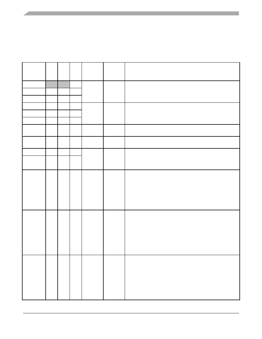
MC56F825x/MC56F824x Digital Signal Controller, Rev. 3
Signal/Connection Descriptions
Freescale Semiconductor
18
3.3
MC56F825x/MC56F824x Signal Pins
After reset, each pin is configured for its primary function (listed first). Any alternative functionality, shown in parentheses and
as italic, must be programmed via the GPIO module’s peripheral enable registers (GPIO_x_PER) and the SIM module’s GPIO
peripheral select (GPSx) registers.
Table 5. MC56F825x/MC56F824x Signal and Package Information
Signal
Name
44
LQFP
48
LQFP
64
LQFP
Type
State
During
Reset
Signal Description
VDD
29
Supply
I/O Power — This pin supplies 3.3 V power to the chip I/O interface.
VDD
29
32
44
VDD
40
44
60
VSS
20
22
30
Supply
I/O Ground — These pins provide ground for chip I/O interface.
VSS
28
31
43
VSS
41
45
61
VDDA
13
15
22
Supply
Analog Power — This pin supplies 3.3 V power to the analog
modules. It must be connected to a clean analog power supply.
VSSA
14
16
23
Supply
Analog Ground — This pin supplies an analog ground to the analog
modules. It must be connected to a clean power supply.
VCAP
17
19
26
Supply
VCAP — Connect a bypass capacitor of 2.2 F or greater between
this pin and VSS to stabilize the core voltage regulator output
required for proper device operation. See Section 8.2, “Electrical
VCAP
39
43
57
TDI
(GPIOD0)
44
48
64
Input
Input/
Output
Input,
internal
pullup
enabled
Test Data Input — This input pin provides a serial input data stream
to the JTAG/EOnCE port. It is sampled on the rising edge of TCK
and has an on-chip pullup resistor.
Port D GPIO — This GPIO pin can be individually programmed as
an input or output pin.
After reset, the default state is TDI.
TDO
(GPIOD1)
42
46
62
Output
Input/
Output
Test Data Output — This tri-stateable output pin provides a serial
output data stream from the JTAG/EOnCE port. It is driven in the
shift-IR and shift-DR controller states, and changes on the falling
edge of TCK.
Port D GPIO — This GPIO pin can be individually programmed as
an input or output pin.
After reset, the default state is TDO.
TCK
(GPIOD2)
111
Input
Input/
Output
Input,
internal
pullup
enabled
Test Clock Input — This input pin provides a gated clock to
synchronize the test logic and shift serial data to the JTAG/EOnCE
port. The pin is connected internally to a pullup resistor. A
Schmitt-trigger input is used for noise immunity.
Port D GPIO — This GPIO pin can be individually programmed as
an input or output pin.
After reset, the default state is TCK
相关PDF资料 |
PDF描述 |
|---|---|
| S9S12P96J0MFT | MCU 96K FLASH AUTO 48-QFN |
| S9S12P64J0MQK | MCU 64K FLASH AUTO 80-QFP |
| S9S12P64J0MLH | MCU 64K FLASH AUTO 64-LQFP |
| VI-2ND-IX-S | CONVERTER MOD DC/DC 85V 75W |
| VI-2NB-IY-B1 | CONVERTER MOD DC/DC 95V 50W |
相关代理商/技术参数 |
参数描述 |
|---|---|
| MC56F8247 | 制造商:FREESCALE 制造商全称:Freescale Semiconductor, Inc 功能描述:Digital Signal Controller Battery chargers and management |
| MC56F8247MLH | 功能描述:数字信号处理器和控制器 - DSP, DSC DSC 64 LQFP 48K FL RoHS:否 制造商:Microchip Technology 核心:dsPIC 数据总线宽度:16 bit 程序存储器大小:16 KB 数据 RAM 大小:2 KB 最大时钟频率:40 MHz 可编程输入/输出端数量:35 定时器数量:3 设备每秒兆指令数:50 MIPs 工作电源电压:3.3 V 最大工作温度:+ 85 C 封装 / 箱体:TQFP-44 安装风格:SMD/SMT |
| MC56F8247VLH | 功能描述:数字信号处理器和控制器 - DSP, DSC DSC 64 LQFP 48K FL RoHS:否 制造商:Microchip Technology 核心:dsPIC 数据总线宽度:16 bit 程序存储器大小:16 KB 数据 RAM 大小:2 KB 最大时钟频率:40 MHz 可编程输入/输出端数量:35 定时器数量:3 设备每秒兆指令数:50 MIPs 工作电源电压:3.3 V 最大工作温度:+ 85 C 封装 / 箱体:TQFP-44 安装风格:SMD/SMT |
| MC56F8247VLHR | 制造商:Freescale Semiconductor 功能描述:MICRO CONTROLLER |
| MC56F824X | 制造商:FREESCALE 制造商全称:Freescale Semiconductor, Inc 功能描述:Digital Signal Controller Battery chargers and management |
发布紧急采购,3分钟左右您将得到回复。