- 您现在的位置:买卖IC网 > PDF目录10991 > MC56F8246VLF (Freescale Semiconductor)DSC 48K FLASH 60MHZ 48-LQFP PDF资料下载
参数资料
| 型号: | MC56F8246VLF |
| 厂商: | Freescale Semiconductor |
| 文件页数: | 46/88页 |
| 文件大小: | 0K |
| 描述: | DSC 48K FLASH 60MHZ 48-LQFP |
| 标准包装: | 250 |
| 系列: | 56F8xxx |
| 核心处理器: | 56800E |
| 芯体尺寸: | 16-位 |
| 速度: | 60MHz |
| 连通性: | CAN,I²C,LIN,SCI,SPI |
| 外围设备: | LVD,POR,PWM,WDT |
| 输入/输出数: | 39 |
| 程序存储器容量: | 48KB(24K x 16) |
| 程序存储器类型: | 闪存 |
| RAM 容量: | 3K x 16 |
| 电压 - 电源 (Vcc/Vdd): | 3 V ~ 3.6 V |
| 数据转换器: | A/D 10x12b,D/A 1x12b |
| 振荡器型: | 内部 |
| 工作温度: | -40°C ~ 105°C |
| 封装/外壳: | 48-LQFP |
| 包装: | 管件 |
第1页第2页第3页第4页第5页第6页第7页第8页第9页第10页第11页第12页第13页第14页第15页第16页第17页第18页第19页第20页第21页第22页第23页第24页第25页第26页第27页第28页第29页第30页第31页第32页第33页第34页第35页第36页第37页第38页第39页第40页第41页第42页第43页第44页第45页当前第46页第47页第48页第49页第50页第51页第52页第53页第54页第55页第56页第57页第58页第59页第60页第61页第62页第63页第64页第65页第66页第67页第68页第69页第70页第71页第72页第73页第74页第75页第76页第77页第78页第79页第80页第81页第82页第83页第84页第85页第86页第87页第88页
MC56F825x/MC56F824x Digital Signal Controller, Rev. 3
Specifications
Freescale Semiconductor
50
7.3
ESD Protection and Latch-up Immunity
Although damage from electrostatic discharge (ESD) is much less common on these devices than on early CMOS circuits, use
normal handling precautions to avoid exposure to static discharge. Qualification tests are performed to ensure that these devices
can withstand exposure to reasonable levels of static without suffering any permanent damage.
All ESD testing conforms with AEC-Q100 Stress Test Qualification. During device qualification, ESD stresses are performed
for the human body model (HBM), the machine model (MM), and the charge device model (CDM).
All latch-up testing conforms with AEC-Q100 Stress Test Qualification.
A device is defined as a failure if, after exposure to ESD pulses, the device no longer meets the device specification.
Comprehensive DC parametric and functional testing is performed according to the applicable device specification at room
temperature and then at hot temperature, unless specified otherwise in the device specification.
7.4
Thermal Characteristics
This section provides information about operating temperature range, power dissipation, and package thermal resistance. Power
dissipation on I/O pins is usually small compared to power dissipation in on-chip logic and voltage regulator circuits, and it is
user-determined rather than being controlled by the device design. To account for PI/O in power calculations, determine the
difference between actual pin voltage and VSS or VDD and multiply by the pin current for each I/O pin. Except in cases of
unusually high pin current (heavy loads), the difference between pin voltage and VSS or VDD is very small.
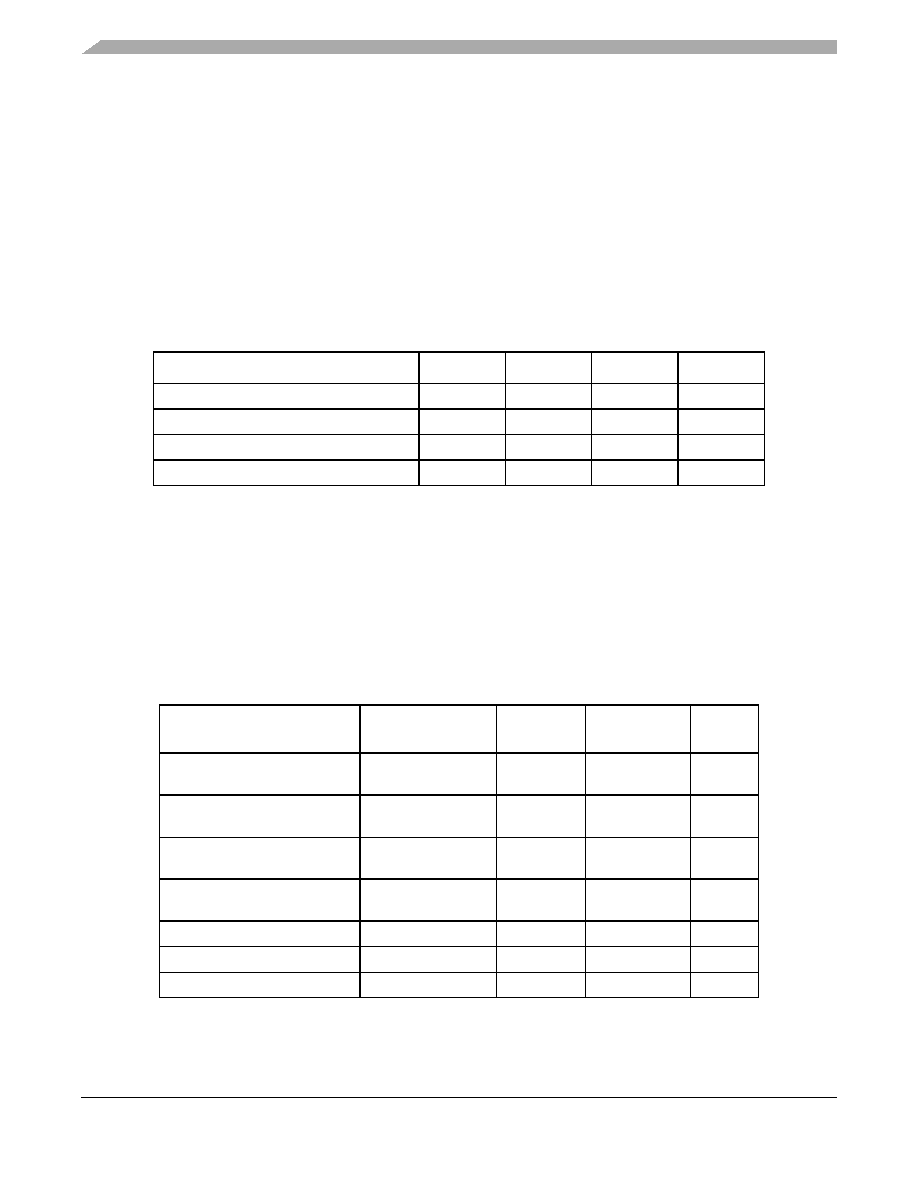
Table 18. MC56F825x/MC56F824x ESD/Latch-up Protection
Characteristic 1
1 Parameter is achieved by design characterization on a small sample size from typical devices under
typical conditions, unless otherwise noted
Min
Typ
Max
Unit
ESD for Human Body Model (HBM)
2000
—
V
ESD for Machine Model (MM)
200
—
V
ESD for Charge Device Model (CDM)
750
—
V
Latch-up current at TA = 85
oC (I
LAT)
± 100
mA
Table 19. 44LQFP Package Thermal Characteristics
Characteristic
Comments
Symbol
Value
(LQFP)
Unit
Junction to ambient
Natural convection
Single layer board
(1s)
RθJA
70
°C/W
Junction to ambient
Natural convection
Four layer board
(2s2p)
RθJMA
48
°C/W
Junction to ambient
(@200 ft/min)
Single layer board
(1s)
RθJMA
57
°C/W
Junction to ambient
(@200 ft/min)
Four layer board
(2s2p)
RθJMA
42
°C/W
Junction to board
RθJB
30
°C/W
Junction to case
RθJC
13
°C/W
Junction to package top
Natural convection
ΨJT
2°C/W
相关PDF资料 |
PDF描述 |
|---|---|
| S9S12P96J0MFT | MCU 96K FLASH AUTO 48-QFN |
| S9S12P64J0MQK | MCU 64K FLASH AUTO 80-QFP |
| S9S12P64J0MLH | MCU 64K FLASH AUTO 64-LQFP |
| VI-2ND-IX-S | CONVERTER MOD DC/DC 85V 75W |
| VI-2NB-IY-B1 | CONVERTER MOD DC/DC 95V 50W |
相关代理商/技术参数 |
参数描述 |
|---|---|
| MC56F8247 | 制造商:FREESCALE 制造商全称:Freescale Semiconductor, Inc 功能描述:Digital Signal Controller Battery chargers and management |
| MC56F8247MLH | 功能描述:数字信号处理器和控制器 - DSP, DSC DSC 64 LQFP 48K FL RoHS:否 制造商:Microchip Technology 核心:dsPIC 数据总线宽度:16 bit 程序存储器大小:16 KB 数据 RAM 大小:2 KB 最大时钟频率:40 MHz 可编程输入/输出端数量:35 定时器数量:3 设备每秒兆指令数:50 MIPs 工作电源电压:3.3 V 最大工作温度:+ 85 C 封装 / 箱体:TQFP-44 安装风格:SMD/SMT |
| MC56F8247VLH | 功能描述:数字信号处理器和控制器 - DSP, DSC DSC 64 LQFP 48K FL RoHS:否 制造商:Microchip Technology 核心:dsPIC 数据总线宽度:16 bit 程序存储器大小:16 KB 数据 RAM 大小:2 KB 最大时钟频率:40 MHz 可编程输入/输出端数量:35 定时器数量:3 设备每秒兆指令数:50 MIPs 工作电源电压:3.3 V 最大工作温度:+ 85 C 封装 / 箱体:TQFP-44 安装风格:SMD/SMT |
| MC56F8247VLHR | 制造商:Freescale Semiconductor 功能描述:MICRO CONTROLLER |
| MC56F824X | 制造商:FREESCALE 制造商全称:Freescale Semiconductor, Inc 功能描述:Digital Signal Controller Battery chargers and management |
发布紧急采购,3分钟左右您将得到回复。