- 您现在的位置:买卖IC网 > PDF目录80459 > MCHC11F1CFNE2 (FREESCALE SEMICONDUCTOR INC) 8-BIT, EEPROM, MICROCONTROLLER, PQCC68 PDF资料下载
参数资料
| 型号: | MCHC11F1CFNE2 |
| 厂商: | FREESCALE SEMICONDUCTOR INC |
| 元件分类: | 微控制器/微处理器 |
| 英文描述: | 8-BIT, EEPROM, MICROCONTROLLER, PQCC68 |
| 封装: | ROHS COMPLIANT AND HALOGEN FREE, PLASTIC, LCC-68 |
| 文件页数: | 32/162页 |
| 文件大小: | 4554K |
| 代理商: | MCHC11F1CFNE2 |
第1页第2页第3页第4页第5页第6页第7页第8页第9页第10页第11页第12页第13页第14页第15页第16页第17页第18页第19页第20页第21页第22页第23页第24页第25页第26页第27页第28页第29页第30页第31页当前第32页第33页第34页第35页第36页第37页第38页第39页第40页第41页第42页第43页第44页第45页第46页第47页第48页第49页第50页第51页第52页第53页第54页第55页第56页第57页第58页第59页第60页第61页第62页第63页第64页第65页第66页第67页第68页第69页第70页第71页第72页第73页第74页第75页第76页第77页第78页第79页第80页第81页第82页第83页第84页第85页第86页第87页第88页第89页第90页第91页第92页第93页第94页第95页第96页第97页第98页第99页第100页第101页第102页第103页第104页第105页第106页第107页第108页第109页第110页第111页第112页第113页第114页第115页第116页第117页第118页第119页第120页第121页第122页第123页第124页第125页第126页第127页第128页第129页第130页第131页第132页第133页第134页第135页第136页第137页第138页第139页第140页第141页第142页第143页第144页第145页第146页第147页第148页第149页第150页第151页第152页第153页第154页第155页第156页第157页第158页第159页第160页第161页第162页
ANALOG-TO-DIGITAL CONVERTER
MOTOROLA
TECHNICAL DATA
10-3
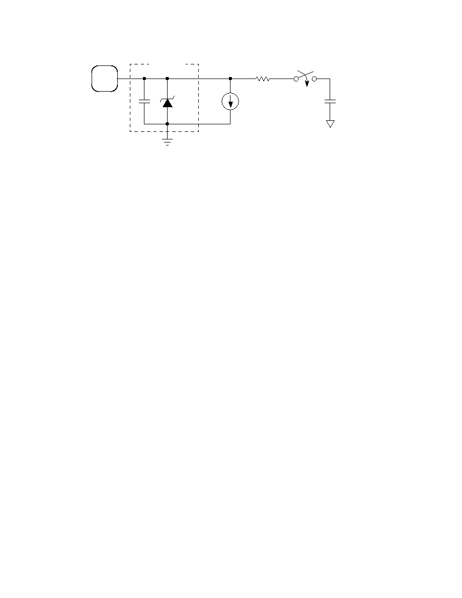
Figure 10-2 Electrical Model of an A/D Input Pin (Sample Mode)
10.1.2 Analog Converter
Conversion of an analog input selected by the multiplexer occurs in this block. It con-
tains a digital-to-analog capacitor (DAC) array, a comparator, and a successive ap-
proximation register (SAR). Each conversion is a sequence of eight comparison
operations, beginning with the most significant bit (MSB). Each comparison deter-
mines the value of a bit in the successive approximation register.
The DAC array performs two functions. It acts as a sample and hold circuit during the
entire conversion sequence, and provides comparison voltage to the comparator dur-
ing each successive comparison.
The result of each successive comparison is stored in the SAR. When a conversion
sequence is complete, the contents of the SAR are transferred to the appropriate re-
sult register.
A charge pump provides switching voltage to the gates of analog switches in the mul-
tiplexer. Charge pump output must stabilize between 7 and 8 volts, thus a delay of up
to 100
s must be imposed after setting ADPU before the converter can be used. The
charge pump is enabled by the ADPU bit in the OPTION register.
Power is provided to the A/D converter system through the AVDD and AVSS pins.
10.1.3 Digital Control
All A/D converter operations are controlled by bits in register ADCTL. In addition to se-
lecting the analog input to be converted, ADCTL bits indicate conversion status, and
control whether single or continuous conversions are performed. Finally, the ADCTL
bits determine whether conversions are performed on single or multiple channels.
10.1.4 Result Registers
Four 8-bit registers (ADR1–ADR4) store conversion results. Each of these registers
can be accessed by the processor in the CPU. The conversion complete flag (CCF)
DAC
CAPACITANCE
VRL
ANALOG
INPUT
PIN
~ 20 pF
+ ~ 20 V
–
~ 0.7 V
< 2 pF
INPUT
PROTECTION
DEVICE
400 nA
JUNCTION
LEAKAGE
DIFFUSION AND
POLY COUPLER
≤ 4 k
* This analog switch is closed only during the 12-cycle sample time.
*
F
re
e
sc
a
le
S
e
m
ic
o
n
d
u
c
to
r,
I
Freescale Semiconductor, Inc.
For More Information On This Product,
Go to: www.freescale.com
n
c
..
.
相关PDF资料 |
PDF描述 |
|---|---|
| MC9S12XEP100VVL | 32-BIT, FLASH, 50 MHz, RISC MICROCONTROLLER, PBGA208 |
| MPC8541CVTAQEX | 32-BIT, 1600 MHz, RISC PROCESSOR, CBGA360 |
| MPC8541ECPXAQEX | 32-BIT, 1420 MHz, RISC PROCESSOR, CBGA360 |
| MC3S12XEP100J1CVL | 32-BIT, FLASH, 50 MHz, RISC MICROCONTROLLER, PBGA208 |
| MIP7365-450F17T | 64-BIT, 450 MHz, MICROPROCESSOR, CQFP208 |
相关代理商/技术参数 |
参数描述 |
|---|---|
| MCHC11F1CFNE2 | 制造商:Freescale Semiconductor 功能描述:8-Bit Microcontroller IC |
| MCHC11F1CFNE2R | 功能描述:8位微控制器 -MCU 8B MCU 1KRAM 512EE RoHS:否 制造商:Silicon Labs 核心:8051 处理器系列:C8051F39x 数据总线宽度:8 bit 最大时钟频率:50 MHz 程序存储器大小:16 KB 数据 RAM 大小:1 KB 片上 ADC:Yes 工作电源电压:1.8 V to 3.6 V 工作温度范围:- 40 C to + 105 C 封装 / 箱体:QFN-20 安装风格:SMD/SMT |
| MCHC11F1CFNE3 | 功能描述:8位微控制器 -MCU 8B MCU 1KRAM 512EE RoHS:否 制造商:Silicon Labs 核心:8051 处理器系列:C8051F39x 数据总线宽度:8 bit 最大时钟频率:50 MHz 程序存储器大小:16 KB 数据 RAM 大小:1 KB 片上 ADC:Yes 工作电源电压:1.8 V to 3.6 V 工作温度范围:- 40 C to + 105 C 封装 / 箱体:QFN-20 安装风格:SMD/SMT |
| MCHC11F1CFNE3 | 制造商:Freescale Semiconductor 功能描述:8-Bit Microcontroller IC |
| MCHC11F1CFNE3R | 功能描述:8位微控制器 -MCU 8B MCU 1KRAM 512EE RoHS:否 制造商:Silicon Labs 核心:8051 处理器系列:C8051F39x 数据总线宽度:8 bit 最大时钟频率:50 MHz 程序存储器大小:16 KB 数据 RAM 大小:1 KB 片上 ADC:Yes 工作电源电压:1.8 V to 3.6 V 工作温度范围:- 40 C to + 105 C 封装 / 箱体:QFN-20 安装风格:SMD/SMT |
发布紧急采购,3分钟左右您将得到回复。