- 您现在的位置:买卖IC网 > PDF目录1952 > MCIMX255AVM4 (Freescale Semiconductor)IC MPU I.MX25 AUTO 400MAPBGA PDF资料下载
参数资料
| 型号: | MCIMX255AVM4 |
| 厂商: | Freescale Semiconductor |
| 文件页数: | 106/140页 |
| 文件大小: | 0K |
| 描述: | IC MPU I.MX25 AUTO 400MAPBGA |
| 标准包装: | 90 |
| 系列: | i.MX25 |
| 核心处理器: | ARM9 |
| 芯体尺寸: | 32-位 |
| 速度: | 400MHz |
| 连通性: | 1 线,CAN,EBI/EMI,以太网,I²C,MMC,智能卡,SPI,SSI,UART/USART,USB OTG |
| 外围设备: | DMA,I²S,LCD,POR,PWM,WDT |
| 输入/输出数: | 128 |
| 程序存储器类型: | 外部程序存储器 |
| RAM 容量: | 144K x 8 |
| 电压 - 电源 (Vcc/Vdd): | 1.15 V ~ 1.52 V |
| 数据转换器: | A/D 3x12b |
| 振荡器型: | 外部 |
| 工作温度: | -40°C ~ 85°C |
| 封装/外壳: | 400-LFBGA |
| 包装: | 托盘 |
第1页第2页第3页第4页第5页第6页第7页第8页第9页第10页第11页第12页第13页第14页第15页第16页第17页第18页第19页第20页第21页第22页第23页第24页第25页第26页第27页第28页第29页第30页第31页第32页第33页第34页第35页第36页第37页第38页第39页第40页第41页第42页第43页第44页第45页第46页第47页第48页第49页第50页第51页第52页第53页第54页第55页第56页第57页第58页第59页第60页第61页第62页第63页第64页第65页第66页第67页第68页第69页第70页第71页第72页第73页第74页第75页第76页第77页第78页第79页第80页第81页第82页第83页第84页第85页第86页第87页第88页第89页第90页第91页第92页第93页第94页第95页第96页第97页第98页第99页第100页第101页第102页第103页第104页第105页当前第106页第107页第108页第109页第110页第111页第112页第113页第114页第115页第116页第117页第118页第119页第120页第121页第122页第123页第124页第125页第126页第127页第128页第129页第130页第131页第132页第133页第134页第135页第136页第137页第138页第139页第140页
i.MX25 Applications Processor for Automotive Products, Rev. 10
68
Freescale Semiconductor
NOTE
For timing purposes, transition to signal high is defined as 80% of signal
value; while signal low is defined as 20% of signal value.
Timing for HCLK is 133 MHz. The internal NFC clock (Flash clock) is
approximately 33 MHz (30 ns). All timings are listed according to this NFC
clock frequency (multiples of NFC clock phases), except NF16 and NF17,
which are not related to the NFC clock.
3.7.6.3
Wireless External Interface Module (WEIM) Timing
(WE1–WE27) shown in the figure.
All WEIM output control signals may be asserted and negated by internal clock relative to BCLK rising
edge or falling edge according to corresponding assertion/negation control fields. Address always begins
relative to BCLK falling edge, but may be ended on rising or falling edge in muxed mode according to the
control register configuration. Output data begins relative to BCLK rising edge except in muxed mode,
where rising or falling edge may be used according to the control register configuration. Input data, ECB
and DTACK are all captured relative to BCLK rising edge.
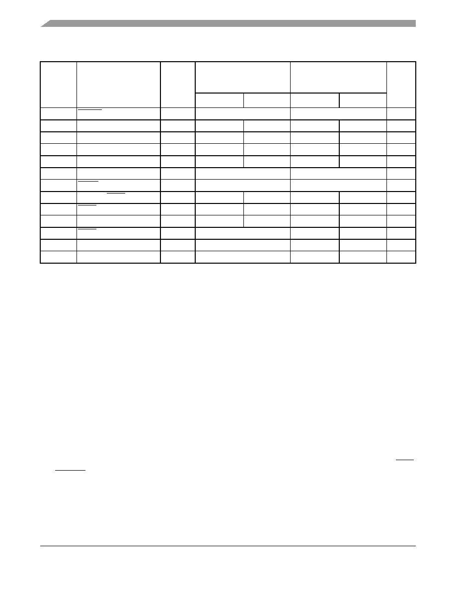
NF5
NF_WP pulse width
tWP
T–1.5 ns
28.5
ns
NF6
NFALE setup time
tALS
T
—
30
—
ns
NF7
NFALE hold time
tALH
T–3.0 ns
—
27
—
ns
NF8
Data setup time
tDS
2T ns
—
60
—
ns
NF9
Data hold time
tDH
T–5.0 ns
—
25
—
ns
NF10
Write cycle time
tWC
2T
60
ns
NF11
NFWE hold time
tWH
T–2.5 ns
27.5
ns
NF12
Ready to NFRE low
tRR
21T–10 ns
—
620
—
ns
NF13
NFRE pulse width
tRP
1.5T
—
45
—
ns
NF14
READ cycle time
tRC
2T
—
60
—
ns
NF15
NFRE high hold time
tREH
0.5T–2.5 ns
12.5
—
ns
NF16
Data setup on read
tDSR
N/A
10
—
ns
NF17
Data hold on read
tDHR
N/A
0
—
ns
1 The Flash clock maximum frequency is 50 MHz.
Table 55. NFC Timing Parameters1 (continued)
ID
Parameter
Symbol
Timing
T = NFC Clock Cycle
Example Timing for
NFC Clock
≈ 33 MHz
T = 30 ns
Unit
Min.
Max.
Min.
Max.
相关PDF资料 |
PDF描述 |
|---|---|
| MCIMX258CJM4A | IC MPU IMX25 IND 400MAPBGA |
| MCIMX27MOP4A | IC MPU I.MX27 19X19 473MAPBGA |
| MCIMX31CVMN4DR2 | IC MPU I.MX31 AUTO 473MAPBGA |
| MCIMX31DVMN5D | IC MPU I.MX31 CONSUMR 473MAPBGA |
| MCIMX31VMN5CR2 | IC MPU MAP I.MX31L 473-MAPBGA |
相关代理商/技术参数 |
参数描述 |
|---|---|
| MCIMX257CJM4 | 功能描述:处理器 - 专门应用 IMX25 INDUSTRIAL RoHS:否 制造商:Freescale Semiconductor 类型:Multimedia Applications 核心:ARM Cortex A9 处理器系列:i.MX6 数据总线宽度:32 bit 最大时钟频率:1 GHz 指令/数据缓存: 数据 RAM 大小:128 KB 数据 ROM 大小: 工作电源电压: 最大工作温度:+ 95 C 安装风格:SMD/SMT 封装 / 箱体:MAPBGA-432 |
| MCIMX257CJM4A | 功能描述:处理器 - 专门应用 IMX25 1.2 INDUST RoHS:否 制造商:Freescale Semiconductor 类型:Multimedia Applications 核心:ARM Cortex A9 处理器系列:i.MX6 数据总线宽度:32 bit 最大时钟频率:1 GHz 指令/数据缓存: 数据 RAM 大小:128 KB 数据 ROM 大小: 工作电源电压: 最大工作温度:+ 95 C 安装风格:SMD/SMT 封装 / 箱体:MAPBGA-432 |
| MCIMX257CJM4A | 制造商:Freescale Semiconductor 功能描述:IC |
| MCIMX257CJN4A | 功能描述:处理器 - 专门应用 12X12 IMX25 1.2 RoHS:否 制造商:Freescale Semiconductor 类型:Multimedia Applications 核心:ARM Cortex A9 处理器系列:i.MX6 数据总线宽度:32 bit 最大时钟频率:1 GHz 指令/数据缓存: 数据 RAM 大小:128 KB 数据 ROM 大小: 工作电源电压: 最大工作温度:+ 95 C 安装风格:SMD/SMT 封装 / 箱体:MAPBGA-432 |
| MCIMX257CVM4 | 功能描述:处理器 - 专门应用 SENNA IMX25 INDUST RoHS:否 制造商:Freescale Semiconductor 类型:Multimedia Applications 核心:ARM Cortex A9 处理器系列:i.MX6 数据总线宽度:32 bit 最大时钟频率:1 GHz 指令/数据缓存: 数据 RAM 大小:128 KB 数据 ROM 大小: 工作电源电压: 最大工作温度:+ 95 C 安装风格:SMD/SMT 封装 / 箱体:MAPBGA-432 |
发布紧急采购,3分钟左右您将得到回复。