- 您现在的位置:买卖IC网 > PDF目录1952 > MCIMX255AVM4 (Freescale Semiconductor)IC MPU I.MX25 AUTO 400MAPBGA PDF资料下载
参数资料
| 型号: | MCIMX255AVM4 |
| 厂商: | Freescale Semiconductor |
| 文件页数: | 123/140页 |
| 文件大小: | 0K |
| 描述: | IC MPU I.MX25 AUTO 400MAPBGA |
| 标准包装: | 90 |
| 系列: | i.MX25 |
| 核心处理器: | ARM9 |
| 芯体尺寸: | 32-位 |
| 速度: | 400MHz |
| 连通性: | 1 线,CAN,EBI/EMI,以太网,I²C,MMC,智能卡,SPI,SSI,UART/USART,USB OTG |
| 外围设备: | DMA,I²S,LCD,POR,PWM,WDT |
| 输入/输出数: | 128 |
| 程序存储器类型: | 外部程序存储器 |
| RAM 容量: | 144K x 8 |
| 电压 - 电源 (Vcc/Vdd): | 1.15 V ~ 1.52 V |
| 数据转换器: | A/D 3x12b |
| 振荡器型: | 外部 |
| 工作温度: | -40°C ~ 85°C |
| 封装/外壳: | 400-LFBGA |
| 包装: | 托盘 |
第1页第2页第3页第4页第5页第6页第7页第8页第9页第10页第11页第12页第13页第14页第15页第16页第17页第18页第19页第20页第21页第22页第23页第24页第25页第26页第27页第28页第29页第30页第31页第32页第33页第34页第35页第36页第37页第38页第39页第40页第41页第42页第43页第44页第45页第46页第47页第48页第49页第50页第51页第52页第53页第54页第55页第56页第57页第58页第59页第60页第61页第62页第63页第64页第65页第66页第67页第68页第69页第70页第71页第72页第73页第74页第75页第76页第77页第78页第79页第80页第81页第82页第83页第84页第85页第86页第87页第88页第89页第90页第91页第92页第93页第94页第95页第96页第97页第98页第99页第100页第101页第102页第103页第104页第105页第106页第107页第108页第109页第110页第111页第112页第113页第114页第115页第116页第117页第118页第119页第120页第121页第122页当前第123页第124页第125页第126页第127页第128页第129页第130页第131页第132页第133页第134页第135页第136页第137页第138页第139页第140页
i.MX25 Applications Processor for Automotive Products, Rev. 10
Freescale Semiconductor
83
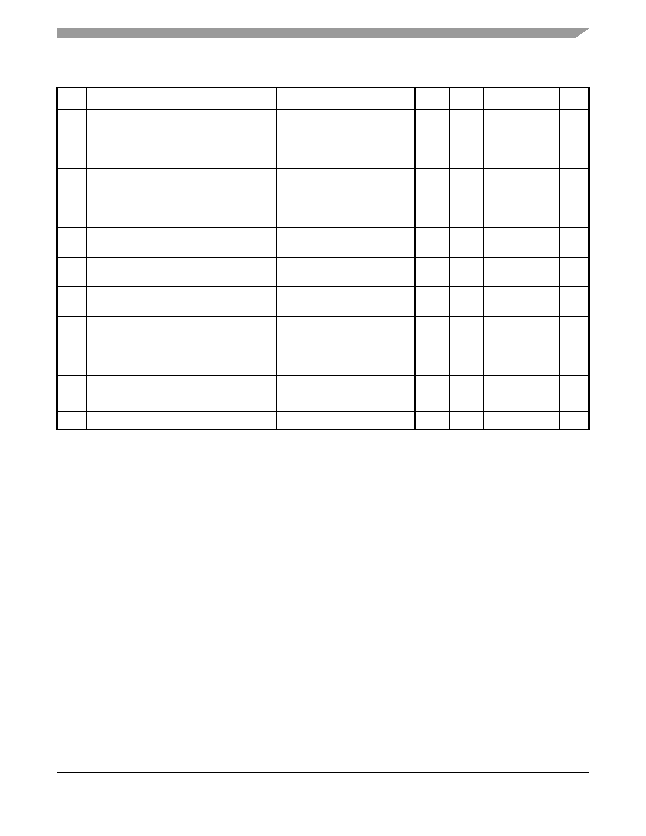
3.7.8
Enhanced Secured Digital Host Controller (eSDHCv2) Timing
figure. The following definitions apply to values and signals described in Table 61:
LS: low-speed mode. Low-speed card can tolerate clocks up to 400 kHz
FS: full-speed mode. Full-speed MMC card’s clock can reach 20 MHz; full speed SD/SDIO card
clock can reach 25 MHz
HS: high-speed mode. High-speed MMC card’s clock can reach 52 MHz; SD/SDIO card clock can
reach 50 MHz
86
SCKT rising edge to data out valid
—
18.0
13.0
x ck
i ck
ns
87
SCKT rising edge to data out high
impedance6
——
—
21.0
16.0
x ck
i ck
ns
88
SCKT rising edge to transmitter #0 drive
enable negation6
——
—
14.0
9.0
x ck
i ck
ns
89
FST input (bl, wr) setup time before SCKT
falling edge5
——
2.0
18.0
—
x ck
i ck
ns
90
FST input (wl) setup time before SCKT falling
edge
——
2.0
18.0
—
x ck
i ck
ns
91
FST input hold time after SCKT falling edge
—
4.0
5.0
—
x ck
i ck
ns
92
FST input (wl) to data out enable from high
impedance
—
21.0
—
ns
93
FST input (wl) to transmitter #0 drive enable
assertion
—
14.0
—
ns
94
Flag output valid after SCKT rising edge
—
14.0
9.0
x ck
i ck
ns
95
HCKR/HCKT clock cycle
—
2 x TC
15
—
ns
96
HCKT input rising edge to SCKT output
—
18.0
—
ns
97
HCKR input rising edge to SCKR output
—
18.0
—
ns
1 V
CORE_VDD = 1.00 ± 0.10 V; TJ = –40 °C to 125 °C, CL = 50 pF
2 In the “Characteristics” column, bl = bit length, wl = word length, wr = word length relative
3 In the “Expression” column, T
C = 7.5 ns.
4 For the internal clock, the external clock cycle is defined by Icyc and the ESAI control register.
5 The word-relative frame sync signal waveform relative to the clock operates in the same manner as the bit-length frame sync
signal waveform, but spreads starting from one serial clock before the first bit clock (same as the bit length frame sync signal),
until the second-to-last bit-clock of the first word in the frame.
6 Periodically sampled and not 100% tested.
Table 60. ESAI General Timing Requirements (continued)
No.
Characteristics1 2
Symbol
Expression3
Min.
Max.
Condition
Unit
相关PDF资料 |
PDF描述 |
|---|---|
| MCIMX258CJM4A | IC MPU IMX25 IND 400MAPBGA |
| MCIMX27MOP4A | IC MPU I.MX27 19X19 473MAPBGA |
| MCIMX31CVMN4DR2 | IC MPU I.MX31 AUTO 473MAPBGA |
| MCIMX31DVMN5D | IC MPU I.MX31 CONSUMR 473MAPBGA |
| MCIMX31VMN5CR2 | IC MPU MAP I.MX31L 473-MAPBGA |
相关代理商/技术参数 |
参数描述 |
|---|---|
| MCIMX257CJM4 | 功能描述:处理器 - 专门应用 IMX25 INDUSTRIAL RoHS:否 制造商:Freescale Semiconductor 类型:Multimedia Applications 核心:ARM Cortex A9 处理器系列:i.MX6 数据总线宽度:32 bit 最大时钟频率:1 GHz 指令/数据缓存: 数据 RAM 大小:128 KB 数据 ROM 大小: 工作电源电压: 最大工作温度:+ 95 C 安装风格:SMD/SMT 封装 / 箱体:MAPBGA-432 |
| MCIMX257CJM4A | 功能描述:处理器 - 专门应用 IMX25 1.2 INDUST RoHS:否 制造商:Freescale Semiconductor 类型:Multimedia Applications 核心:ARM Cortex A9 处理器系列:i.MX6 数据总线宽度:32 bit 最大时钟频率:1 GHz 指令/数据缓存: 数据 RAM 大小:128 KB 数据 ROM 大小: 工作电源电压: 最大工作温度:+ 95 C 安装风格:SMD/SMT 封装 / 箱体:MAPBGA-432 |
| MCIMX257CJM4A | 制造商:Freescale Semiconductor 功能描述:IC |
| MCIMX257CJN4A | 功能描述:处理器 - 专门应用 12X12 IMX25 1.2 RoHS:否 制造商:Freescale Semiconductor 类型:Multimedia Applications 核心:ARM Cortex A9 处理器系列:i.MX6 数据总线宽度:32 bit 最大时钟频率:1 GHz 指令/数据缓存: 数据 RAM 大小:128 KB 数据 ROM 大小: 工作电源电压: 最大工作温度:+ 95 C 安装风格:SMD/SMT 封装 / 箱体:MAPBGA-432 |
| MCIMX257CVM4 | 功能描述:处理器 - 专门应用 SENNA IMX25 INDUST RoHS:否 制造商:Freescale Semiconductor 类型:Multimedia Applications 核心:ARM Cortex A9 处理器系列:i.MX6 数据总线宽度:32 bit 最大时钟频率:1 GHz 指令/数据缓存: 数据 RAM 大小:128 KB 数据 ROM 大小: 工作电源电压: 最大工作温度:+ 95 C 安装风格:SMD/SMT 封装 / 箱体:MAPBGA-432 |
发布紧急采购,3分钟左右您将得到回复。