- 您现在的位置:买卖IC网 > PDF目录69032 > MCIMX514AJM6C (FREESCALE SEMICONDUCTOR INC) SPECIALTY MICROPROCESSOR CIRCUIT, PBGA529 PDF资料下载
参数资料
| 型号: | MCIMX514AJM6C |
| 厂商: | FREESCALE SEMICONDUCTOR INC |
| 元件分类: | 微控制器/微处理器 |
| 英文描述: | SPECIALTY MICROPROCESSOR CIRCUIT, PBGA529 |
| 封装: | 19 X 19 MM, 0.8 MM PITCH, ROHS COMPLIANT, BGA-529 |
| 文件页数: | 114/172页 |
| 文件大小: | 2218K |
| 代理商: | MCIMX514AJM6C |
第1页第2页第3页第4页第5页第6页第7页第8页第9页第10页第11页第12页第13页第14页第15页第16页第17页第18页第19页第20页第21页第22页第23页第24页第25页第26页第27页第28页第29页第30页第31页第32页第33页第34页第35页第36页第37页第38页第39页第40页第41页第42页第43页第44页第45页第46页第47页第48页第49页第50页第51页第52页第53页第54页第55页第56页第57页第58页第59页第60页第61页第62页第63页第64页第65页第66页第67页第68页第69页第70页第71页第72页第73页第74页第75页第76页第77页第78页第79页第80页第81页第82页第83页第84页第85页第86页第87页第88页第89页第90页第91页第92页第93页第94页第95页第96页第97页第98页第99页第100页第101页第102页第103页第104页第105页第106页第107页第108页第109页第110页第111页第112页第113页当前第114页第115页第116页第117页第118页第119页第120页第121页第122页第123页第124页第125页第126页第127页第128页第129页第130页第131页第132页第133页第134页第135页第136页第137页第138页第139页第140页第141页第142页第143页第144页第145页第146页第147页第148页第149页第150页第151页第152页第153页第154页第155页第156页第157页第158页第159页第160页第161页第162页第163页第164页第165页第166页第167页第168页第169页第170页第171页第172页
i.MX51A Automotive and Infotainment Applications Processors, Rev. 4
46
Freescale Semiconductor
Electrical Characteristics
4.6.5
DPLL Electrical Parameters
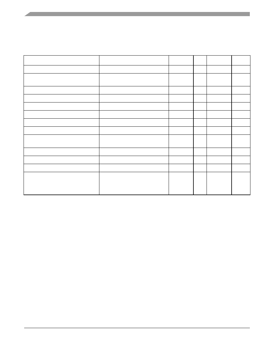
Table 48 shows the DPLL electical parameters.
4.6.6
NAND Flash Controller (NFC) Parameters
This section provides the relative timing requirements among different signals of NFC at the module level
in the different operational modes.
Timing parameters in Figure 14, through Figure 17, Figure 19, and Table 50 show the default NFC mode
(asymmetric mode) using two Flash clock cycles per one access of RE_B and WE_B.
Timing parameters in Figure 14, Figure 15, Figure 16, Figure 18, Figure 19, and Table 50 show symmetric
NFC mode using one Flash clock cycle per one access of RE_B and WE_B.
Table 48. DPLL Electrical Parameters
Parameter
Test Conditions/Remarks
Min
Typ
Max
Unit
Reference clock frequency range1
1 Device input range cannot exceed the electrical specifications of the CAMP, see Table 47.
—
10
—
100
MHz
Reference clock frequency range after
pre-divider
—10
—
40
MHz
Output clock frequency range (dpdck_2)
—
300
—
1025
MHz
Pre-division factor2
2 The values specified here are internal to DPLL. Inside the DPLL, a “1” is added to the value specified by the user.Therefore,
the user has to enter a value “1” less than the desired value at the inputs of DPLL for PDF and MFD.
—1
—
16
—
Multiplication factor integer part
—
5
—
15
—
Multiplication factor numerator3
3 The maximum total multiplication factor (MFI + MFN/MFD) allowed is 15.Therefore, if the MFI value is 15, MFN value must be
zero.
Should be less than denominator
–67108862
—
67108862
—
Multiplication factor denominator2
—
1
—
67108863
—
Output Duty Cycle
—
48.5
50
51.5
%
Frequency lock time4
(FOL mode or non-integer MF)
4 T
dpdref is the time period of the reference clock after predivider.According to the specification, the maximum lock time in FOL
mode is 398 cycles of divided reference clock when DPLL starts after full reset.
——
—
398
Tdpdref
Phase lock time
—
100
s
Frequency jitter5 (peak value)
5 Tdck is the time period of the output clock, dpdck_2.
—
0.02
0.04
Tdck
Phase jitter (peak value)
FPL mode, integer and fractional MF
—
2.0
3.5
ns
Power dissipation
fdck = 300 MHz @ avdd = 1.8 V,
dvdd = 1.2 V
fdck = 650 MHz @ avdd = 1.8 V,
dvdd = 1.2 V
—
0.65 (avdd)
0.92 (dvdd)
1.98 (avdd)
1.8 (dvdd)
mW
相关PDF资料 |
PDF描述 |
|---|---|
| MCIMX537CVV8C | 32-BIT, 800 MHz, RISC PROCESSOR, PBGA529 |
| MCM16Y1BACFT16 | 16-BIT, MROM, MICROCONTROLLER, PQFP160 |
| MCM16Y1BGCFT16 | 16-BIT, MROM, MICROCONTROLLER, PQFP160 |
| M68HC16Y1CFC | 16-BIT, MROM, MICROCONTROLLER, PQFP16 |
| MCV14AI/SL | 8-BIT, FLASH, 20 MHz, RISC MICROCONTROLLER, PDSO14 |
相关代理商/技术参数 |
参数描述 |
|---|---|
| MCIMX514AJM6CR2 | 制造商:Freescale Semiconductor 功能描述:ELVIS 3.0 AUTO - Tape and Reel |
| MCIMX515CJM6C | 功能描述:处理器 - 专门应用 iMX515 App Processor RoHS:否 制造商:Freescale Semiconductor 类型:Multimedia Applications 核心:ARM Cortex A9 处理器系列:i.MX6 数据总线宽度:32 bit 最大时钟频率:1 GHz 指令/数据缓存: 数据 RAM 大小:128 KB 数据 ROM 大小: 工作电源电压: 最大工作温度:+ 95 C 安装风格:SMD/SMT 封装 / 箱体:MAPBGA-432 |
| MCIMX515CJM6CR2 | 功能描述:处理器 - 专门应用 i.MX51 32bit 800 MHz RoHS:否 制造商:Freescale Semiconductor 类型:Multimedia Applications 核心:ARM Cortex A9 处理器系列:i.MX6 数据总线宽度:32 bit 最大时钟频率:1 GHz 指令/数据缓存: 数据 RAM 大小:128 KB 数据 ROM 大小: 工作电源电压: 最大工作温度:+ 95 C 安装风格:SMD/SMT 封装 / 箱体:MAPBGA-432 |
| MCIMX515DJM8C | 功能描述:处理器 - 专门应用 iMX515 App Processor Extended Temp RoHS:否 制造商:Freescale Semiconductor 类型:Multimedia Applications 核心:ARM Cortex A9 处理器系列:i.MX6 数据总线宽度:32 bit 最大时钟频率:1 GHz 指令/数据缓存: 数据 RAM 大小:128 KB 数据 ROM 大小: 工作电源电压: 最大工作温度:+ 95 C 安装风格:SMD/SMT 封装 / 箱体:MAPBGA-432 |
| MCIMX515DJM8C | 制造商:Freescale Semiconductor 功能描述:; LEADED PROCESS COMPATIBLE:YES; PEAK RE |
发布紧急采购,3分钟左右您将得到回复。