- 您现在的位置:买卖IC网 > PDF目录67997 > ML9041-XXBCVWA (LAPIS SEMICONDUCTOR CO LTD) 17 X 100 DOTS DOT MAT LCD DRVR AND DSPL CTLR, UUC175 PDF资料下载
参数资料
| 型号: | ML9041-XXBCVWA |
| 厂商: | LAPIS SEMICONDUCTOR CO LTD |
| 元件分类: | 显示控制器 |
| 英文描述: | 17 X 100 DOTS DOT MAT LCD DRVR AND DSPL CTLR, UUC175 |
| 封装: | 10.62 X 2.55 MM, GOLD BUMP, DIE-175 |
| 文件页数: | 45/61页 |
| 文件大小: | 572K |
| 代理商: | ML9041-XXBCVWA |
第1页第2页第3页第4页第5页第6页第7页第8页第9页第10页第11页第12页第13页第14页第15页第16页第17页第18页第19页第20页第21页第22页第23页第24页第25页第26页第27页第28页第29页第30页第31页第32页第33页第34页第35页第36页第37页第38页第39页第40页第41页第42页第43页第44页当前第45页第46页第47页第48页第49页第50页第51页第52页第53页第54页第55页第56页第57页第58页第59页第60页第61页
PEDL9041-03
1Semiconductor
ML9041-xxA/xxB
4/60
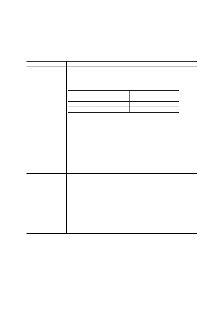
PIN DESCRIPTIONS
Symbol
Description
R/W
The input pin with a pull-up resistor to select Read (“H”) or Write (“L”) in the Parallel I/F
Mode.
This pin should be open in the Serial l/F Mode.
RS
0, RS1
The input pins with a pull-up resistor to select a register in the Parallel l/F Mode.
This pin should be open in the Serial I/F Mode.
E
The input pin for data input/output between the CPU and the ML9041 and for
activating instructions in the Parallel l/F Mode.
This pin should be open in the Serial l/F Mode.
DB
0 to DB3
The input/output pins to transfer data of lower-order 4 bits between the CPU and the
ML9041 in the Parallel l/F Mode. The pins are not used for the 4-bit interface and
serial interface.
Each pin is equipped with a pull-up resistor, so this pin should be open when not used.
DB
4 to DB7
The input/output pins to transfer data of upper 4 bits between the CPU and the
ML9041 in the Parallel l/F Mode. The pins are not used for the serial interface.
Each pin is equipped with a pull-up resistor, so this pin should be open in the Serial I/F
Mode when not used.
OSC
1
OSC
2
OSC
R
The clock oscillation pins required for LCD drive signals and the operation of the
ML9041 by instructions sent from the CPU.
To input external clock, the OSC
1 pin should be used. The OSCR and the OSC2 pins
should be open.
To start oscillation with an external resistor, the resistor should be connected between
the OSC
1 and OSC2 pins. The OSCR pin should be open.
To start oscillation with an internal resistor, the OSC
2 and OSCR pins should be
short-circuited outside the ML9041. The OSC
1 pin should be open.
COM
1 to COM17
The LCD common signal output pins.
For 1/9 duty, non-selectable voltage waveforms are output via COM
10 to COM17. For
1/12 duty, non-selectable voltage waveforms are output via COM
13 to COM17.
SEG
1 to SEG100
The LCD segment signal output pins.
RS
1
RS
0
Name of register
H
Data register
H
L
Instruction register
L
Expansion Instruction register
相关PDF资料 |
PDF描述 |
|---|---|
| ML9206-XXGA | 36 X 16 DOTS DOT MAT LCD DRVR AND DSPL CTLR, PQFP64 |
| ML9206-01GA | 36 X 16 DOTS DOT MAT LCD DRVR AND DSPL CTLR, PQFP64 |
| MM66307SP/FP | LV/LV-A/LVX/H SERIES, 16-BIT DRIVER, TRUE OUTPUT, PDSO32 |
| MM908E625ACDWB/R2 | 8-BIT, FLASH, 8 MHz, MICROCONTROLLER, PDSO54 |
| MMBD701L | SILICON, VHF-UHF BAND, MIXER DIODE, TO-236AB |
相关代理商/技术参数 |
参数描述 |
|---|---|
| ML9042 | 制造商:OKI 制造商全称:OKI electronic componets 功能描述:DOT MATRIX LCD CONTROLLER DRIVER |
| ML9042-54CVWA-5016 | 制造商:ROHM Semiconductor 功能描述:RHOML9042-54CVWA-5016 OKI LCD DRIVER |
| ML9044 | 制造商:OKI 制造商全称:OKI electronic componets 功能描述:DOT MATRIX LCD CONTROLLER DRIVER |
| ML9044A | 制造商:OKI 制造商全称:OKI electronic componets 功能描述:DOT MATRIX LCD CONTROLLER DRIVER |
| ML9044A-XXACVWA | 制造商:OKI 制造商全称:OKI electronic componets 功能描述:DOT MATRIX LCD CONTROLLER DRIVER |
发布紧急采购,3分钟左右您将得到回复。