- 您现在的位置:买卖IC网 > PDF目录182950 > MM908E621 (飞思卡尔半导体(中国)有限公司) Integrated Quad Half-Bridge and Triple High-Side with Embedded MCU and LIN for High End Mirror PDF资料下载
参数资料
| 型号: | MM908E621 |
| 厂商: | 飞思卡尔半导体(中国)有限公司 |
| 英文描述: | Integrated Quad Half-Bridge and Triple High-Side with Embedded MCU and LIN for High End Mirror |
| 中文描述: | 综合四半桥和三高的嵌入式微控制器和LIN高端侧镜 |
| 文件页数: | 41/62页 |
| 文件大小: | 719K |
| 代理商: | MM908E621 |
第1页第2页第3页第4页第5页第6页第7页第8页第9页第10页第11页第12页第13页第14页第15页第16页第17页第18页第19页第20页第21页第22页第23页第24页第25页第26页第27页第28页第29页第30页第31页第32页第33页第34页第35页第36页第37页第38页第39页第40页当前第41页第42页第43页第44页第45页第46页第47页第48页第49页第50页第51页第52页第53页第54页第55页第56页第57页第58页第59页第60页第61页第62页
Analog Integrated Circuit Device Data
46
Freescale Semiconductor
908E621
Functional Device Operation
Logic Commands and Registers
LOGIC COMMANDS AND REGISTERS
908E621 SERIAL PHERIPHERAL INTERFACE (SPI)
The Serial Peripheral Interface (SPI) creates the
communication link between the MCU and the analog die.
The interface consists of four terminals
MOSI - Master Out Slave In (internal pull-down)
MISO - Master In Slave Out
SPSCK - Serial Clock (internal pull-down)
SS - Slave Select (internal pull-up)
A complete data transfer via the SPI, consists of 2 bytes.
The master sends address and data, the slave returns
system status and the data of the selected address.
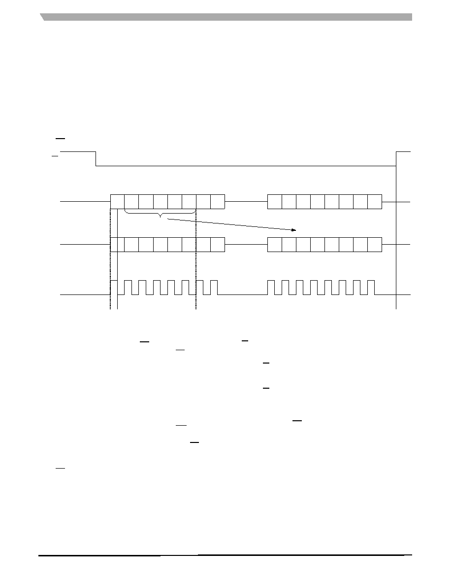
Figure 29. SPI Protocol
During the inactive phase of SS, the new data transfer
will be prepared. The falling edge on the SS line,
indicates the start of a new data transfer (framing) and
puts MISO in the low impedance mode. The first valid
data are moved to MISO with the rising edge of SPSCK.
The MOSI, MISO will change data on a rising edge of
SPSCK.
The MOSI, MISO will be sampled on a falling edge of
SPSCK.
The data transfer is only valid, if exactly 16 sample clock
edges are present in the active phase of SS.
After a write operation the transmitted data will be
latched into the register, by the rising edge of SS.
Register read data is internally latched into the SPI, at
the time when the parity bit is transferred
SS high will force MISO to high impedance
Master Address Byte
A4 - A0
include the address of the desired register.
R/W
includes the information if it is a read or a write operation.
If R/W = 1 (read operation), second byte of master
contains no valid information, slave just transmits back
register data.
If R/W = 0 (write operation), master sends data to be
written in the second byte, slave sends concurrently
contents of selected register prior to write operation,
write data is latched in the SmartMOS registers on
rising edge of SS
Parity P
completes the total number of 1 bits of (R/W,A[4-0]) to an
even number. e.g. (R/W,A[4-0]) = 100001 -> P0 = 0.
The parity bit is only evaluated during a write operations
and ignored for read operations.
Bit X
not used
S7
S6
S5
S4
S3
S2
S1
S0
R/W
A4
A3
A2
A1
A0
P
X
D7
D6
D5
D4
D3
D2
D1
D0
D7
D6
D5
D4
D3
D2
D1
D0
System Status Register
Read/Write, Address, Parity
Data (Register write)
Data (Register read)
Rising edge of SPSCK
Change MISO/MOSI
Output
Falling edge of SPSCK
Sample MISO/MOSI
Input
Slave latch
register address
Slave latch
data
SS
MOSI
MISO
SPSCK
相关PDF资料 |
PDF描述 |
|---|---|
| MM9329-2700TB1 | BOARD TERMINATED, FEMALE, RF CONNECTOR, SURFACE MOUNT, RECEPTACLE |
| MXTK92XX1001 | INTERCONNECTION DEVICE |
| MM9329-2700TB2 | BOARD TERMINATED, FEMALE, RF CONNECTOR, SURFACE MOUNT, RECEPTACLE |
| MM121480 | CABLE TERMINATED, FEMALE-MALE, RF STRAIGHT ADAPTER, JACK |
| MM121470 | CABLE TERMINATED, FEMALE-FEMALE, RF STRAIGHT ADAPTER, JACK |
相关代理商/技术参数 |
参数描述 |
|---|---|
| MM908E621_08 | 制造商:FREESCALE 制造商全称:Freescale Semiconductor, Inc 功能描述:Integrated Quad Half-bridge and Triple High Side with Embedded MCU and LIN for High End Mirror |
| MM908E621ACDWB | 功能描述:8位微控制器 -MCU QUAD H-B/3-HS W/MCU & LI RoHS:否 制造商:Silicon Labs 核心:8051 处理器系列:C8051F39x 数据总线宽度:8 bit 最大时钟频率:50 MHz 程序存储器大小:16 KB 数据 RAM 大小:1 KB 片上 ADC:Yes 工作电源电压:1.8 V to 3.6 V 工作温度范围:- 40 C to + 105 C 封装 / 箱体:QFN-20 安装风格:SMD/SMT |
| MM908E621ACDWB/R2 | 制造商:FREESCALE 制造商全称:Freescale Semiconductor, Inc 功能描述:Integrated Quad Half-bridge and Triple High Side with Embedded MCU and LIN for High End Mirror |
| MM908E621ACDWBR2 | 功能描述:8位微控制器 -MCU QUAD HB / TRIPLE HS 841B RoHS:否 制造商:Silicon Labs 核心:8051 处理器系列:C8051F39x 数据总线宽度:8 bit 最大时钟频率:50 MHz 程序存储器大小:16 KB 数据 RAM 大小:1 KB 片上 ADC:Yes 工作电源电压:1.8 V to 3.6 V 工作温度范围:- 40 C to + 105 C 封装 / 箱体:QFN-20 安装风格:SMD/SMT |
| MM908E621ACPEK | 功能描述:8位微控制器 -MCU QUAD H-B/3-HS W/MCU & LI RoHS:否 制造商:Silicon Labs 核心:8051 处理器系列:C8051F39x 数据总线宽度:8 bit 最大时钟频率:50 MHz 程序存储器大小:16 KB 数据 RAM 大小:1 KB 片上 ADC:Yes 工作电源电压:1.8 V to 3.6 V 工作温度范围:- 40 C to + 105 C 封装 / 箱体:QFN-20 安装风格:SMD/SMT |
发布紧急采购,3分钟左右您将得到回复。