- 您现在的位置:买卖IC网 > PDF目录1954 > MM908E621ACDWBR2 (Freescale Semiconductor)IC SW QUAD HB/TRPL HISID 54-SOIC PDF资料下载
参数资料
| 型号: | MM908E621ACDWBR2 |
| 厂商: | Freescale Semiconductor |
| 文件页数: | 24/60页 |
| 文件大小: | 0K |
| 描述: | IC SW QUAD HB/TRPL HISID 54-SOIC |
| 标准包装: | 1,000 |
| 应用: | 自动镜像控制 |
| 核心处理器: | HC08 |
| 程序存储器类型: | 闪存(16 kB) |
| 控制器系列: | 908E |
| RAM 容量: | 512 x 8 |
| 接口: | SCI,SPI |
| 输入/输出数: | 12 |
| 电源电压: | 9 V ~ 16 V |
| 工作温度: | -40°C ~ 85°C |
| 安装类型: | 表面贴装 |
| 封装/外壳: | 54-BSSOP(0.295",7.50mm 宽)裸露焊盘 |
| 包装: | 带卷 (TR) |
| 供应商设备封装: | 54-SOICW-EP |
第1页第2页第3页第4页第5页第6页第7页第8页第9页第10页第11页第12页第13页第14页第15页第16页第17页第18页第19页第20页第21页第22页第23页当前第24页第25页第26页第27页第28页第29页第30页第31页第32页第33页第34页第35页第36页第37页第38页第39页第40页第41页第42页第43页第44页第45页第46页第47页第48页第49页第50页第51页第52页第53页第54页第55页第56页第57页第58页第59页第60页
Analog Integrated Circuit Device Data
30
Freescale Semiconductor
908E621
FUNCTIONAL DEVICE OPERATION
OPERATIONAL MODES
1 = Wake-up due to L0 pin
0 = no Wake-up due to L0 pin
ANALOG DIE INPUTS/OUTPUTS
LIN PHYSICAL LAYER
The LIN bus pin provides a physical layer for single wire
communication in automotive applications. The LIN physical
layer is designed to meet the LIN physical layer specification.
The LIN driver is a low side MOSFET with internal current
limitation and thermal shutdown. An internal pull-up resistor
with a serial diode structure is integrated, so no external pull-
up components are required for the application in a slave
node. The fall time from dominant to recessive and the rise
time from recessive to dominant is controlled. The symmetry
between both slew rate controls is guaranteed.
The slew rate can be selected for optimized operation at
10 and 20 kBit/s as well as high baud rates for test and
programming. The slew rate can be adapted with 2 bits
SRS[1:0] in the System Control Register. The initial slew rate
is optimized for 20 kBit/s.
The LIN pin offers high susceptibility immunity level from
external disturbance, guaranteeing communication during
external disturbance.
The LIN transmitter circuitry is enabled by setting the
PSON bit in the System Control Register (SYSCTL).
If the transmitter works in the current limitation region, the
LINCL bit in the System Status Register (SYSSTAT) is set
and the LIN transceiver is disabled after a certain time.
For improved performance and safe behavior, in case of
LIN bus short to Ground or LIN bus leakage during low power
mode, the internal pull-up resistor on the LIN pin is
disconnected from VSUP and a small current source keeps
the LIN bus at recessive level. In case of a LIN bus short to
GND, this feature will reduce the current consumption in
STOP and SLEEP modes.
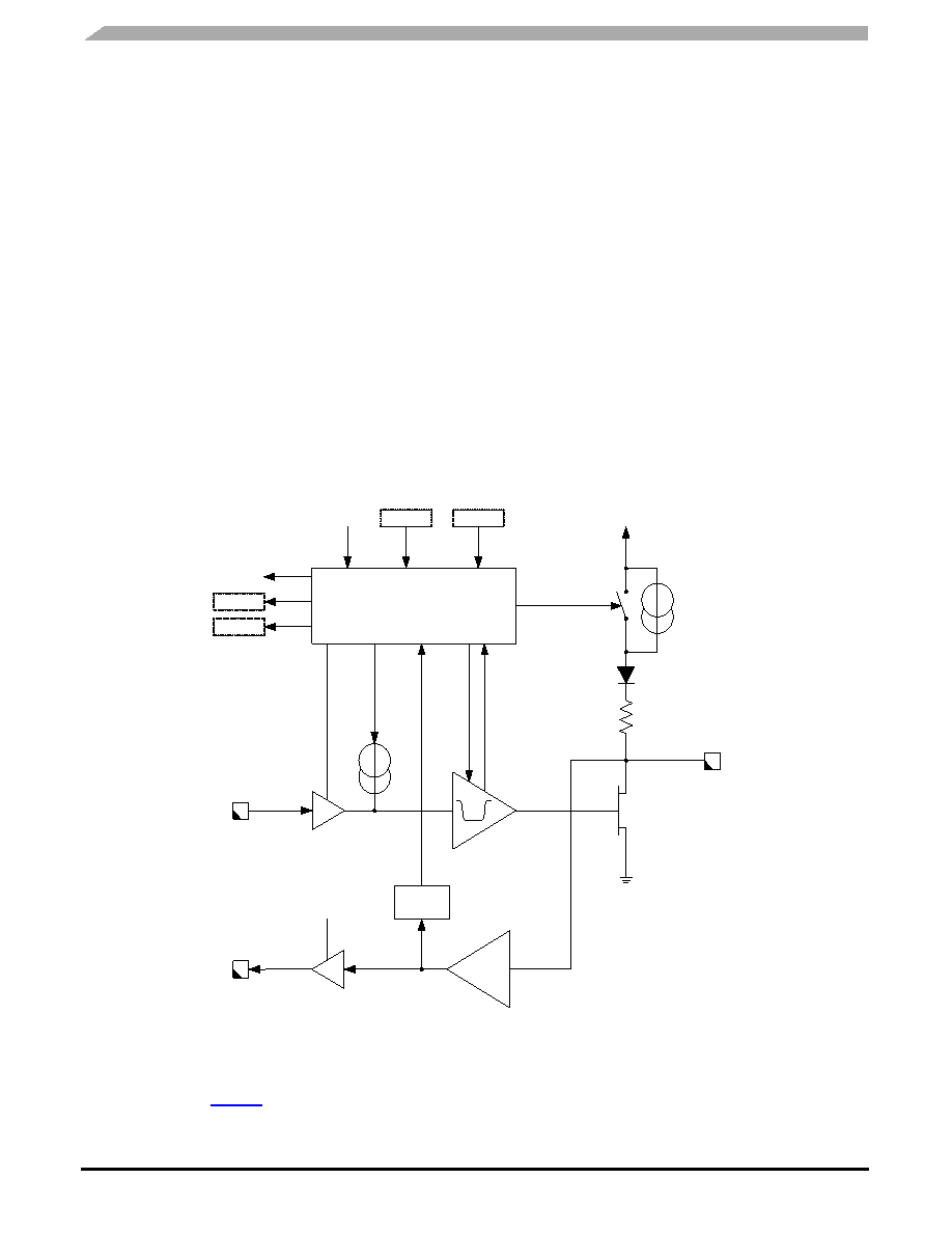
Figure 16. LIN Interface
TXD Pin
The TXD pin is the MCU interface to control the state of the
LIN transmitter (see Figure 2). When TXD is LOW, the LIN
pin is low (dominant state). When TXD is HIGH, the LIN
output MOSFET is turned off (recessive state). The TXD pin
has an internal pull-up current source to set the LIN bus to a
recessive state in the event, for instance, if the
Control
Receiv
er
Wake-up
RXD
TXD
GND
VSUP
Slope
Control
30k
10A
LIN bus
SRS[1:0]
PSON
LINCL
LINIF
Wake-up
Filter
MODE
TESTMODE
相关PDF资料 |
PDF描述 |
|---|---|
| MM908E622ACEK | IC HALF-BRIDGE QUAD 54-SOIC |
| MM908E624ACEWR2 | IC SWITCH TRPL HI MCU/LIN 54SOIC |
| MM908E625ACDWB | IC QUAD HALF BRDG MCU/LIN 54SOIC |
| MM908E626AVDWB | IC STEPPER MOTOR DRIVER 54-SOIC |
| MM912F634BV1AER2 | IC MCU 16BIT 32KB FLASH 48LQFP |
相关代理商/技术参数 |
参数描述 |
|---|---|
| MM908E621ACPEK | 功能描述:8位微控制器 -MCU QUAD H-B/3-HS W/MCU & LI RoHS:否 制造商:Silicon Labs 核心:8051 处理器系列:C8051F39x 数据总线宽度:8 bit 最大时钟频率:50 MHz 程序存储器大小:16 KB 数据 RAM 大小:1 KB 片上 ADC:Yes 工作电源电压:1.8 V to 3.6 V 工作温度范围:- 40 C to + 105 C 封装 / 箱体:QFN-20 安装风格:SMD/SMT |
| MM908E621ACPEKR2 | 功能描述:8位微控制器 -MCU QUAD HB AND TRIPLE HS RoHS:否 制造商:Silicon Labs 核心:8051 处理器系列:C8051F39x 数据总线宽度:8 bit 最大时钟频率:50 MHz 程序存储器大小:16 KB 数据 RAM 大小:1 KB 片上 ADC:Yes 工作电源电压:1.8 V to 3.6 V 工作温度范围:- 40 C to + 105 C 封装 / 箱体:QFN-20 安装风格:SMD/SMT |
| MM908E622 | 制造商:FREESCALE 制造商全称:Freescale Semiconductor, Inc 功能描述:Integrated Quad Half-Bridge, Triple High-Side and EC Glass Driver with Embedded MCU and LIN for High End Mirror |
| MM908E622_08 | 制造商:FREESCALE 制造商全称:Freescale Semiconductor, Inc 功能描述:Integrated Quad Half-bridge, Triple High Side and EC Glass Driver with Embedded MCU and LIN for High End Mirror |
| MM908E622ACDR2 | 制造商:FREESCALE 制造商全称:Freescale Semiconductor, Inc 功能描述:Integrated Quad Half-Bridge, Triple High-Side and EC Glass Driver with Embedded MCU and LIN for High End Mirror |
发布紧急采购,3分钟左右您将得到回复。