- 您现在的位置:买卖IC网 > PDF目录17046 > MPC8323E-RDB (Freescale Semiconductor)BOARD REFERENCE DESIGN PDF资料下载
参数资料
| 型号: | MPC8323E-RDB |
| 厂商: | Freescale Semiconductor |
| 文件页数: | 6/82页 |
| 文件大小: | 0K |
| 描述: | BOARD REFERENCE DESIGN |
| 产品培训模块: | MPC8323E PowerQUICC II Pro Processor |
| 标准包装: | 1 |
| 系列: | PowerQUICC II™ PRO |
| 类型: | MCU |
| 适用于相关产品: | MPC8323E |
| 所含物品: | 参考设计板、软件和说明文档 |
| 相关产品: | MPC8323CVRADDC-ND - IC MPU PWRQUICC II 516-PBGA MPC8323CVRAFDC-ND - IC MPU PWRQUICC II 516-PBGA MPC8323CZQADDC-ND - IC MPU PWRQUICC II 516-PBGA MPC8323CZQAFDC-ND - IC MPU PWRQUICC II 516-PBGA MPC8323ECVRAFDC-ND - IC MPU PWRQUICC II 516-PBGA MPC8323ECVRADDC-ND - IC MPU PWRQUICC II 516-PBGA MPC8323ZQAFDC-ND - IC MPU PWRQUICC II 516-PBGA MPC8323ZQADDC-ND - IC MPU PWRQUICC II 516-PBGA MPC8323VRADDC-ND - IC MPU PWRQUICC II 516-PBGA MPC8323EZQAFDC-ND - IC MPU POWERQUICC II 516-PBGA 更多... |
第1页第2页第3页第4页第5页当前第6页第7页第8页第9页第10页第11页第12页第13页第14页第15页第16页第17页第18页第19页第20页第21页第22页第23页第24页第25页第26页第27页第28页第29页第30页第31页第32页第33页第34页第35页第36页第37页第38页第39页第40页第41页第42页第43页第44页第45页第46页第47页第48页第49页第50页第51页第52页第53页第54页第55页第56页第57页第58页第59页第60页第61页第62页第63页第64页第65页第66页第67页第68页第69页第70页第71页第72页第73页第74页第75页第76页第77页第78页第79页第80页第81页第82页
MPC8323E PowerQUICC II Pro Integrated Communications Processor Family Hardware Specifications, Rev. 4
14
Freescale Semiconductor
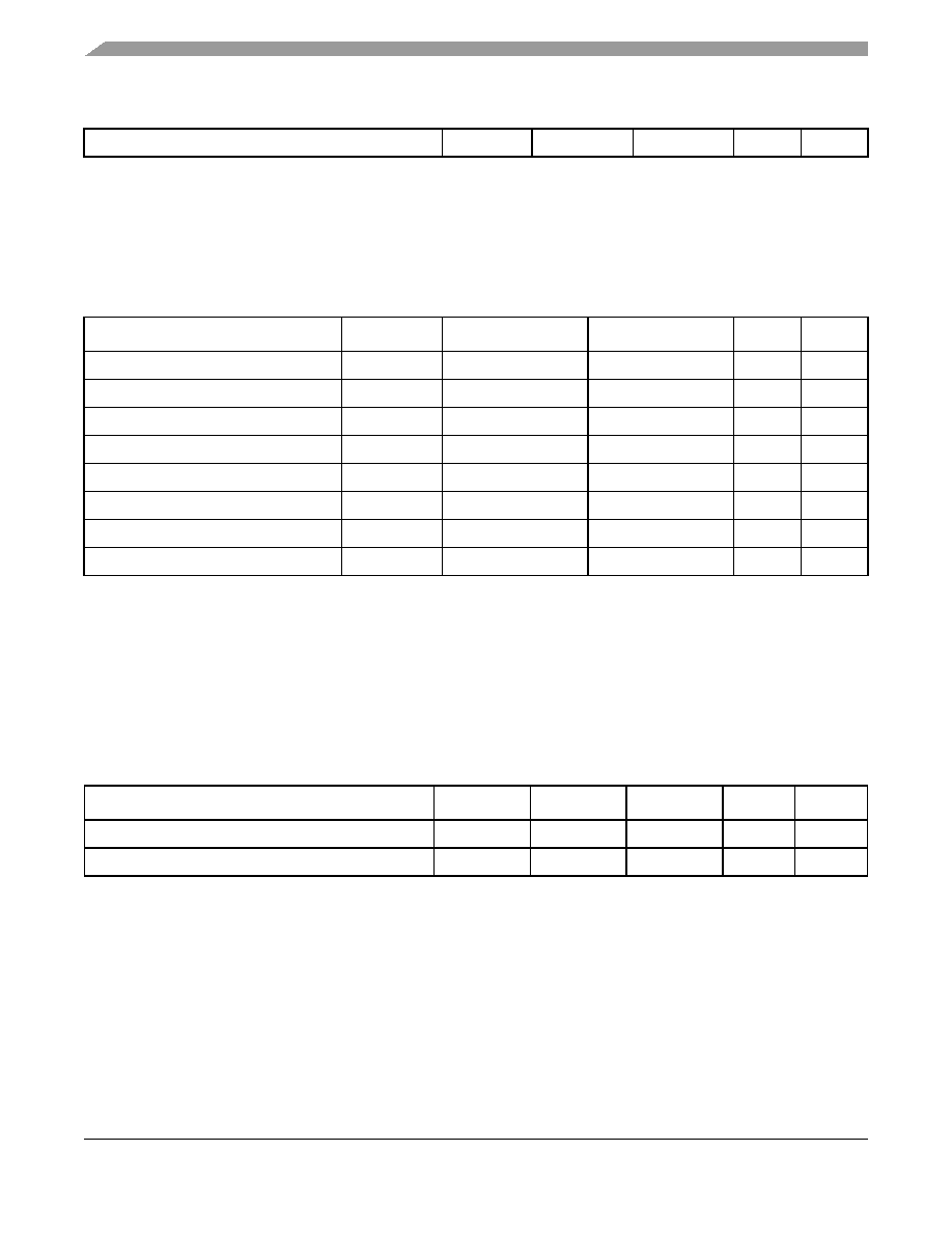
DDR1 and DDR2 SDRAM
Table 14 provides the recommended operating conditions for the DDR1 SDRAM component(s) of the
MPC8323E when Dn_GVDD(typ) = 2.5 V.
Delta input/output capacitance: DQ, DQS
CDIO
—0.5
pF
1
Note:
1. This parameter is sampled. D
n
_GVDD = 1.8 V ± 0.090 V, f = 1 MHz, TA =25°C, VOUT = Dn_GVDD ÷ 2,
VOUT (peak-to-peak) = 0.2 V.
Table 14. DDR1 SDRAM DC Electrical Characteristics for D
n
_GVDD(typ) = 2.5 V
Parameter/Condition
Symbol
Min
Max
Unit
Notes
I/O supply voltage
D
n
_GVDD
2.375
2.625
V
1
I/O reference voltage
MVREF
nREF
0.49
× Dn_GVDD
0.51
× Dn_GVDD
V2
I/O termination voltage
VTT
MVREF
nREF – 0.04
MVREF
nREF + 0.04
V
3
Input high voltage
VIH
MVREF
nREF + 0.15
D
n
_GVDD + 0.3
V
—
Input low voltage
VIL
–0.3
MVREF
nREF – 0.15
V
—
Output leakage current
IOZ
–9.9
μA4
Output high current (VOUT = 1.95 V)
IOH
–16.2
—
mA
—
Output low current (VOUT = 0.35 V)
IOL
16.2
—
mA
—
Notes:
1. D
n
_GVDD is expected to be within 50 mV of the DRAM Dn_GVDD at all times.
2. MVREF
nREF is expected to be equal to 0.5 × Dn_GVDD, and to track Dn_GVDD DC variations as measured at the receiver.
Peak-to-peak noise on MVREF
nREF may not exceed ±2% of the DC value.
3. VTT is not applied directly to the device. It is the supply to which far end signal termination is made and is expected to be
equal to MVREF
nREF. This rail should track variations in the DC level of MVREFnREF.
4. Output leakage is measured with all outputs disabled, 0 V
≤ VOUT ≤ Dn_GVDD.
Table 15. DDR1 SDRAM Capacitance for D
n
_GVDD(typ) = 2.5 V Interface
Parameter/Condition
Symbol
Min
Max
Unit
Notes
Input/output capacitance: DQ,DQS
CIO
68
pF
1
Delta input/output capacitance: DQ, DQS
CDIO
—0.5
pF
1
Note:
1. This parameter is sampled. D
n
_GVDD = 2.5 V ± 0.125 V, f = 1 MHz, TA = 25° C, VOUT = Dn_GVDD ÷ 2,
VOUT (peak-to-peak) = 0.2 V.
Table 13. DDR2 SDRAM Capacitance for D
n
_GVDD(typ) = 1.8 V
相关PDF资料 |
PDF描述 |
|---|---|
| GMC05DRAH-S734 | CONN EDGECARD 10POS .100 R/A SLD |
| RBC13DCST-S288 | CONN EDGECARD 26POS .100 EXTEND |
| STD02W-G | WIRE & CABLE MARKERS |
| STD01W-V | WIRE & CABLE MARKERS |
| 0210490187 | CABLE JUMPER 1.25MM .305M 12POS |
相关代理商/技术参数 |
参数描述 |
|---|---|
| MPC8323E-RDB | 制造商:Freescale Semiconductor 功能描述:MPC8323E Integrated Multiservice Gateway |
| MPC8323EVRADDC | 功能描述:微处理器 - MPU 8323 NOPB PBGA W/ENC RoHS:否 制造商:Atmel 处理器系列:SAMA5D31 核心:ARM Cortex A5 数据总线宽度:32 bit 最大时钟频率:536 MHz 程序存储器大小:32 KB 数据 RAM 大小:128 KB 接口类型:CAN, Ethernet, LIN, SPI,TWI, UART, USB 工作电源电压:1.8 V to 3.3 V 最大工作温度:+ 85 C 安装风格:SMD/SMT 封装 / 箱体:FBGA-324 |
| MPC8323EVRADDCA | 制造商:Freescale Semiconductor 功能描述:POWERQUICC, 32 BIT POWER ARCHITECTURE SOC, 266MHZ E300, QE, - Trays 制造商:Freescale Semiconductor 功能描述:IC MPU PWRQUICC 266MHZ 516BGA |
| MPC8323EVRAFDC | 功能描述:微处理器 - MPU 8323 NOPB PBGA W/ENC RoHS:否 制造商:Atmel 处理器系列:SAMA5D31 核心:ARM Cortex A5 数据总线宽度:32 bit 最大时钟频率:536 MHz 程序存储器大小:32 KB 数据 RAM 大小:128 KB 接口类型:CAN, Ethernet, LIN, SPI,TWI, UART, USB 工作电源电压:1.8 V to 3.3 V 最大工作温度:+ 85 C 安装风格:SMD/SMT 封装 / 箱体:FBGA-324 |
| MPC8323EVRAFDCA | 制造商:FREESCALE 制造商全称:Freescale Semiconductor, Inc 功能描述:PowerQUICC? II Pro Integrated Communications Processor Family Hardware Specifications |
发布紧急采购,3分钟左右您将得到回复。