- 您现在的位置:买卖IC网 > PDF目录17039 > MPC8379E-MDS-PB (Freescale Semiconductor)BOARD PROCESSOR FOR MDS S PDF资料下载
参数资料
| 型号: | MPC8379E-MDS-PB |
| 厂商: | Freescale Semiconductor |
| 文件页数: | 24/117页 |
| 文件大小: | 0K |
| 描述: | BOARD PROCESSOR FOR MDS S |
| 标准包装: | 1 |
| 系列: | PowerQUICC II™ PRO |
| 类型: | MPU |
| 适用于相关产品: | MPC8379 |
| 所含物品: | 板 |
第1页第2页第3页第4页第5页第6页第7页第8页第9页第10页第11页第12页第13页第14页第15页第16页第17页第18页第19页第20页第21页第22页第23页当前第24页第25页第26页第27页第28页第29页第30页第31页第32页第33页第34页第35页第36页第37页第38页第39页第40页第41页第42页第43页第44页第45页第46页第47页第48页第49页第50页第51页第52页第53页第54页第55页第56页第57页第58页第59页第60页第61页第62页第63页第64页第65页第66页第67页第68页第69页第70页第71页第72页第73页第74页第75页第76页第77页第78页第79页第80页第81页第82页第83页第84页第85页第86页第87页第88页第89页第90页第91页第92页第93页第94页第95页第96页第97页第98页第99页第100页第101页第102页第103页第104页第105页第106页第107页第108页第109页第110页第111页第112页第113页第114页第115页第116页第117页
MPC8379E PowerQUICC II Pro Processor Hardware Specifications, Rev. 8
14
Freescale Semiconductor
4.2
AC Electrical Characteristics
The primary clock source for the device can be one of two inputs, CLKIN or PCI_CLK, depending on
whether the device is configured in PCI host or PCI agent mode. This table provides the clock input
(CLKIN/PCI_CLK) AC timing specifications for the device.
4.3
eTSEC Gigabit Reference Clock Timing
This table provides the eTSEC gigabit reference clocks (EC_GTX_CLK125) AC timing specifications.
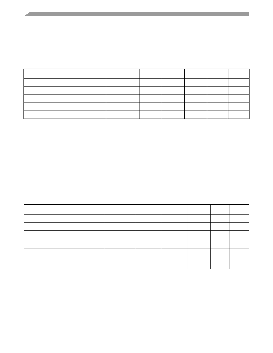
Table 8. CLKIN AC Timing Specifications
Parameter
Symbol
Min
Typical
Max
Unit
Note
CLKIN/PCI_CLK frequency
fCLKIN
25
—
66.666
MHz
CLKIN/PCI_CLK cycle time
tCLKIN
15
—
40
ns
—
CLKIN/PCI_CLK rise and fall time
tKH, tKL
0.6
1.0
2.3
ns
CLKIN/PCI_CLK duty cycle
tKHK/tCLKIN
40
—
60
%
CLKIN/PCI_CLK jitter
—
± 150
ps
Notes:
1. Caution: The system, core and security block must not exceed their respective maximum or minimum operating
frequencies.
2. Rise and fall times for CLKIN/PCI_CLK are measured at 0.4 V and 2.7 V.
3. Timing is guaranteed by design and characterization.
4. This represents the total input jitter-short term and long term-and is guaranteed by design.
5. The CLKIN/PCI_CLK driver’s closed loop jitter bandwidth should be < 500 kHz at –20 dB. The bandwidth must be set low
to allow cascade-connected PLL-based devices to track CLKIN drivers with the specified jitter.
6. Spread spectrum is allowed up to 1% down-spread on CLKIN/PCI_CLK up to 60 KHz.
Table 9. EC_GTX_CLK125 AC Timing Specifications
At recommended operating conditions with LVDD = 2.5 ± 0.125 mV/ 3.3 V ± 165 mV
Parameter/Condition
Symbol
Min
Typical
Max
Unit
Note
EC_GTX_CLK125 frequency
tG125
—
125
—
MHz
—
EC_GTX_CLK125 cycle time
tG125
—8
—
ns
—
EC_GTX_CLK rise and fall time
LVDD = 2.5 V
LVDD = 3.3 V
tG125R/tG125F
——
0.75
1.0
ns
EC_GTX_CLK125 duty cycle
1000Base-T for RGMII, RTBI
tG125H/tG125
47
—
53
EC_GTX_CLK125 jitter
—
±150
ps
Notes:
1. Rise and fall times for EC_GTX_CLK125 are measured from 0.5 and 2.0 V for LVDD = 2.5 V and from 0.6 and 2.7 V for
LVDD =3.3 V.
2. EC_GTX_CLK125 is used to generate the GTX clock for the eTSEC transmitter with 2% degradation. The
EC_GTX_CLK125 duty cycle can be loosened from 47%/ 53% as long as the PHY device can tolerate the duty cycle
generated by the eTSEC GTX_CLK. See Section 8.2.2, “RGMII and RTBI AC Timing Specifications,” for the duty cycle for
10Base-T and 100Base-T reference clock.
相关PDF资料 |
PDF描述 |
|---|---|
| MPC8378E-MDS-PB | BOARD PROCESSOR FOR MDS S |
| MPC5553EVBE | BOARD EVAL FOR MPC5553 |
| MPC8323E-MDS-PB | BOARD MODULE DEV SYSTEM 8323 |
| MPC5534EVBE | BOARD EVAL FOR MPC5534 |
| MPC8313E-RDBB | BOARD CPU 8313E VER 2.1 |
相关代理商/技术参数 |
参数描述 |
|---|---|
| MPC8379E-RDB | 功能描述:网络控制器与处理器 IC REF BRD FOR MPC837 RoHS:否 制造商:Micrel 产品:Controller Area Network (CAN) 收发器数量: 数据速率: 电源电流(最大值):595 mA 最大工作温度:+ 85 C 安装风格:SMD/SMT 封装 / 箱体:PBGA-400 封装:Tray |
| MPC8379E-RDBA | 功能描述:开发板和工具包 - 其他处理器 MPC8379E REF DESIGN BD RoHS:否 制造商:Freescale Semiconductor 产品:Development Systems 工具用于评估:P3041 核心:e500mc 接口类型:I2C, SPI, USB 工作电源电压: |
| MPC8379E-RDBA | 制造商:Freescale Semiconductor 功能描述:MPC8379E-RDB Reference Platform |
| MPC8379EVRAFDA | 制造商:FREESCALE 制造商全称:Freescale Semiconductor, Inc 功能描述:PowerQUICC? II Pro Processor Hardware Specifications |
| MPC8379EVRAFFA | 制造商:FREESCALE 制造商全称:Freescale Semiconductor, Inc 功能描述:PowerQUICC? II Pro Processor Hardware Specifications |
发布紧急采购,3分钟左右您将得到回复。