- 您现在的位置:买卖IC网 > PDF目录17039 > MPC8379E-MDS-PB (Freescale Semiconductor)BOARD PROCESSOR FOR MDS S PDF资料下载
参数资料
| 型号: | MPC8379E-MDS-PB |
| 厂商: | Freescale Semiconductor |
| 文件页数: | 31/117页 |
| 文件大小: | 0K |
| 描述: | BOARD PROCESSOR FOR MDS S |
| 标准包装: | 1 |
| 系列: | PowerQUICC II™ PRO |
| 类型: | MPU |
| 适用于相关产品: | MPC8379 |
| 所含物品: | 板 |
第1页第2页第3页第4页第5页第6页第7页第8页第9页第10页第11页第12页第13页第14页第15页第16页第17页第18页第19页第20页第21页第22页第23页第24页第25页第26页第27页第28页第29页第30页当前第31页第32页第33页第34页第35页第36页第37页第38页第39页第40页第41页第42页第43页第44页第45页第46页第47页第48页第49页第50页第51页第52页第53页第54页第55页第56页第57页第58页第59页第60页第61页第62页第63页第64页第65页第66页第67页第68页第69页第70页第71页第72页第73页第74页第75页第76页第77页第78页第79页第80页第81页第82页第83页第84页第85页第86页第87页第88页第89页第90页第91页第92页第93页第94页第95页第96页第97页第98页第99页第100页第101页第102页第103页第104页第105页第106页第107页第108页第109页第110页第111页第112页第113页第114页第115页第116页第117页
MPC8379E PowerQUICC II Pro Processor Hardware Specifications, Rev. 8
20
Freescale Semiconductor
The minimum frequency for DDR2 is 250 MHz data rate (125 MHz clock), 167 MHz data rate (83 MHz
clock) for DDR1. This figure shows the DDR1 and DDR2 SDRAM output timing for the MCK to MDQS
skew measurement (tDDKHMH).
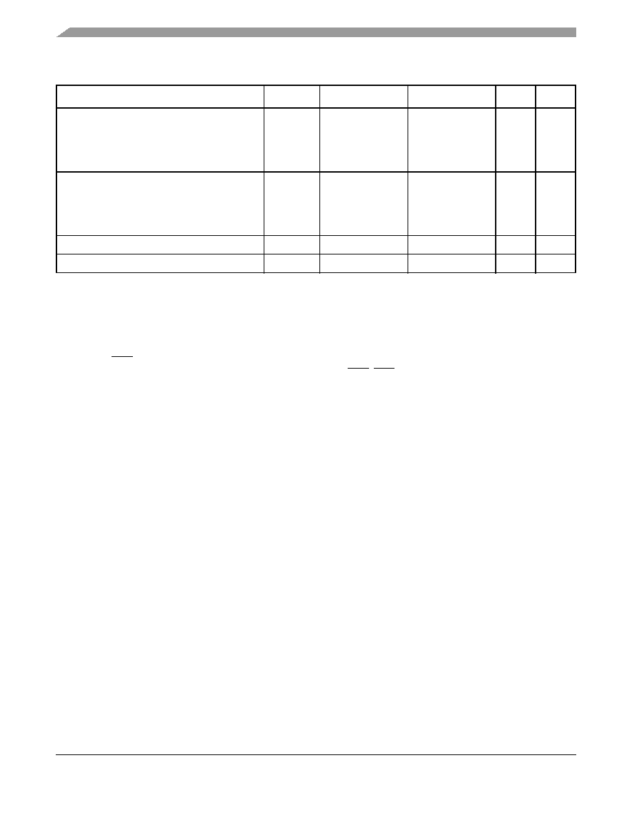
MDQ//MDM output setup with respect to MDQS
400 MHz data rate
333 MHz data rate
266 MHz data rate
200 MHz data rate
tDDKHDS,
tDDKLDS
550
800
1100
1200
—
ps
MDQ//MDM output hold with respect to MDQS
400 MHz data rate
333 MHz data rate
266 MHz data rate
200 MHz data rate
tDDKHDX,
tDDKLDX
700
800
1100
1200
—
ps
MDQS preamble start
tDDKHMP
–0.5
× tMCK –0.6
–0.5
× tMCK + 0.6
ns
MDQS epilogue end
tDDKHME
–0.6
0.6
ns
Notes:
1. The symbols used for timing specifications follow the pattern of t(first two letters of functional block)(signal)(state) (reference)(state) for
inputs and t(first two letters of functional block)(reference)(state)(signal)(state) for outputs. Output hold time can be read as DDR timing
(DD) from the rising or falling edge of the reference clock (KH or KL) until the output went invalid (AX or DX). For example,
tDDKHAS symbolizes DDR timing (DD) for the time tMCK memory clock reference (K) goes from the high (H) state until
outputs (A) are setup (S) or output valid time. Also, tDDKLDX symbolizes DDR timing (DD) for the time tMCK memory clock
reference (K) goes low (L) until data outputs (D) are invalid (X) or data output hold time.
2. All MCK/MCK referenced measurements are made from the crossing of the two signals ±0.1 V.
3. ADDR/CMD includes all DDR SDRAM output signals except MCK/MCK, MCS, and MDQ//MDM/MDQS.
4. Note that tDDKHMH follows the symbol conventions described in Note 1. For example, tDDKHMH describes the DDR timing
(DD) from the rising edge of the MCK[n] clock (KH) until the MDQS signal is valid (MH). tDDKHMH can be modified through
control of the DQSS override bits in the TIMING_CFG_2 register. This will typically be set to the same delay as the clock
adjust in the CLK_CNTL register. The timing parameters listed in the table assume that these 2 parameters have been set
to the same adjustment value. See the
MPC8379E PowerQUICC II Pro Host Processor Reference Manual for a description
and understanding of the timing modifications enabled by use of these bits.
5. Determined by maximum possible skew between a data strobe (MDQS) and any corresponding bit of data MDQ, ECC, or
data mask (MDM). The data strobe should be centered inside of the data eye at the pins of the microprocessor.
6. All outputs are referenced to the rising edge of MCK
n at the pins of the microprocessor. Note that tDDKHMP follows the
symbol conventions described in Note 1.
7. Clock Control register is set to adjust the memory clocks by 1/2 the applied cycle.
8. See AN3665, “MPC837xE Design Checklist,” for proper DDR termination.
Table 21. DDR1 and DDR2 SDRAM Output AC Timing Specifications (continued)
Parameter
Symbol1
Min
Max
Unit
Note
相关PDF资料 |
PDF描述 |
|---|---|
| MPC8378E-MDS-PB | BOARD PROCESSOR FOR MDS S |
| MPC5553EVBE | BOARD EVAL FOR MPC5553 |
| MPC8323E-MDS-PB | BOARD MODULE DEV SYSTEM 8323 |
| MPC5534EVBE | BOARD EVAL FOR MPC5534 |
| MPC8313E-RDBB | BOARD CPU 8313E VER 2.1 |
相关代理商/技术参数 |
参数描述 |
|---|---|
| MPC8379E-RDB | 功能描述:网络控制器与处理器 IC REF BRD FOR MPC837 RoHS:否 制造商:Micrel 产品:Controller Area Network (CAN) 收发器数量: 数据速率: 电源电流(最大值):595 mA 最大工作温度:+ 85 C 安装风格:SMD/SMT 封装 / 箱体:PBGA-400 封装:Tray |
| MPC8379E-RDBA | 功能描述:开发板和工具包 - 其他处理器 MPC8379E REF DESIGN BD RoHS:否 制造商:Freescale Semiconductor 产品:Development Systems 工具用于评估:P3041 核心:e500mc 接口类型:I2C, SPI, USB 工作电源电压: |
| MPC8379E-RDBA | 制造商:Freescale Semiconductor 功能描述:MPC8379E-RDB Reference Platform |
| MPC8379EVRAFDA | 制造商:FREESCALE 制造商全称:Freescale Semiconductor, Inc 功能描述:PowerQUICC? II Pro Processor Hardware Specifications |
| MPC8379EVRAFFA | 制造商:FREESCALE 制造商全称:Freescale Semiconductor, Inc 功能描述:PowerQUICC? II Pro Processor Hardware Specifications |
发布紧急采购,3分钟左右您将得到回复。