- 您现在的位置:买卖IC网 > PDF目录3935 > MPC8544EAVTAQGA (Freescale Semiconductor)IC MPU POWERQUICC III 783-FCBGA PDF资料下载
参数资料
| 型号: | MPC8544EAVTAQGA |
| 厂商: | Freescale Semiconductor |
| 文件页数: | 64/117页 |
| 文件大小: | 0K |
| 描述: | IC MPU POWERQUICC III 783-FCBGA |
| 标准包装: | 36 |
| 系列: | MPC85xx |
| 处理器类型: | 32-位 MPC85xx PowerQUICC III |
| 速度: | 1.0GHz |
| 电压: | 0.95 V ~ 1.05 V |
| 安装类型: | 表面贴装 |
| 封装/外壳: | 783-BBGA,FCBGA |
| 供应商设备封装: | 783-FCPBGA(29x29) |
| 包装: | 托盘 |
第1页第2页第3页第4页第5页第6页第7页第8页第9页第10页第11页第12页第13页第14页第15页第16页第17页第18页第19页第20页第21页第22页第23页第24页第25页第26页第27页第28页第29页第30页第31页第32页第33页第34页第35页第36页第37页第38页第39页第40页第41页第42页第43页第44页第45页第46页第47页第48页第49页第50页第51页第52页第53页第54页第55页第56页第57页第58页第59页第60页第61页第62页第63页当前第64页第65页第66页第67页第68页第69页第70页第71页第72页第73页第74页第75页第76页第77页第78页第79页第80页第81页第82页第83页第84页第85页第86页第87页第88页第89页第90页第91页第92页第93页第94页第95页第96页第97页第98页第99页第100页第101页第102页第103页第104页第105页第106页第107页第108页第109页第110页第111页第112页第113页第114页第115页第116页第117页
MPC8544E PowerQUICC III Integrated Processor Hardware Specifications, Rev. 6
50
Freescale Semiconductor
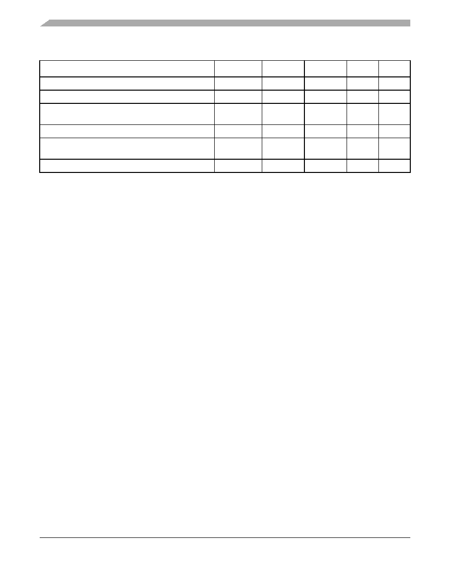
Local Bus
Local bus clock to data valid for LAD/LDP
tLBKLOV2
—
1.6
ns
4
Local bus clock to address valid for LAD, and LALE
tLBKLOV3
—
1.6
ns
4
Output hold from local bus clock (except LAD/LDP and
LALE)
tLBKLOX1
–4.1
—
ns
4
Output hold from local bus clock for LAD/LDP
tLBKLOX2
–4.1
—
ns
4
Local bus clock to output high Impedance (except
LAD/LDP and LALE)
tLBKLOZ1
—
1.4
ns
7
Local bus clock to output high impedance for LAD/LDP
tLBKLOZ2
—
1.4
ns
7
Notes:
1. The symbols used for timing specifications follow the pattern of t(first two letters of functional block)(signal)(state)(reference)(state) for
inputs and t(first two letters of functional block)(reference)(state)(signal)(state) for outputs. For example, tLBIXKH1 symbolizes local bus
timing (LB) for the input (I) to go invalid (X) with respect to the time the tLBK clock reference (K) goes high (H), in this case
for clock one (1). Also, tLBKHOX symbolizes local bus timing (LB) for the tLBK clock reference (K) to go high (H), with respect
to the output (O) going invalid (X) or output hold time.
2. All timings are in reference to local bus clock for PLL bypass mode. Timings may be negative with respect to the local bus
clock because the actual launch and capture of signals is done with the internal launch/capture clock, which proceeds LCLK
by tLBKHKT.
3. Maximum possible clock skew between a clock LCLK[m] and a relative clock LCLK[n]. Skew measured between
complementary signals at BVDD/2.
4. All signals are measured from BVDD/2 of the rising edge of local bus clock for PLL bypass mode to 0.4 × BVDD of the signal
in question for 3.3-V signaling levels.
5. Input timings are measured at the pin.
6. The value of tLBOTOT is the measurement of the minimum time between the negation of LALE and any change in LAD.
7. For purposes of active/float timing measurements, the Hi-Z or off state is defined to be when the total current delivered
through the component pin is less than or equal to the leakage current specification.
Table 48. Local Bus General Timing Parameters—PLL Bypassed (continued)
Parameter
Symbol1
Min
Max
Unit
Notes
相关PDF资料 |
PDF描述 |
|---|---|
| MPC8544EAVTANGA | IC MPU POWERQUICC III 783-FCBGA |
| MPC8544EAVTALFA | IC MPU POWERQUICC III 783-FCBGA |
| SLW5S-5C7LF | CONN ZIF CIC 5POS DIP 1MM VERT |
| XF2L-0735-1A | CONNECTOR FPC 7POS 0.5MM SMD |
| XF2L-0725-1A | CONN FPC 7POS 0.5MM PITCH SMD |
相关代理商/技术参数 |
参数描述 |
|---|---|
| MPC8544EAVTARJ | 功能描述:微处理器 - MPU PQ3 8544E Netwrk Comm Indstrl Cntrl RoHS:否 制造商:Atmel 处理器系列:SAMA5D31 核心:ARM Cortex A5 数据总线宽度:32 bit 最大时钟频率:536 MHz 程序存储器大小:32 KB 数据 RAM 大小:128 KB 接口类型:CAN, Ethernet, LIN, SPI,TWI, UART, USB 工作电源电压:1.8 V to 3.3 V 最大工作温度:+ 85 C 安装风格:SMD/SMT 封装 / 箱体:FBGA-324 |
| MPC8544EAVTARJA | 功能描述:数字信号处理器和控制器 - DSP, DSC PQ38K 8544E RoHS:否 制造商:Microchip Technology 核心:dsPIC 数据总线宽度:16 bit 程序存储器大小:16 KB 数据 RAM 大小:2 KB 最大时钟频率:40 MHz 可编程输入/输出端数量:35 定时器数量:3 设备每秒兆指令数:50 MIPs 工作电源电压:3.3 V 最大工作温度:+ 85 C 封装 / 箱体:TQFP-44 安装风格:SMD/SMT |
| MPC8544ECVTALF | 功能描述:微处理器 - MPU PQ38K 8544E RoHS:否 制造商:Atmel 处理器系列:SAMA5D31 核心:ARM Cortex A5 数据总线宽度:32 bit 最大时钟频率:536 MHz 程序存储器大小:32 KB 数据 RAM 大小:128 KB 接口类型:CAN, Ethernet, LIN, SPI,TWI, UART, USB 工作电源电压:1.8 V to 3.3 V 最大工作温度:+ 85 C 安装风格:SMD/SMT 封装 / 箱体:FBGA-324 |
| MPC8544ECVTALFA | 功能描述:数字信号处理器和控制器 - DSP, DSC PQ38K 8544E COMMERCIAL RoHS:否 制造商:Microchip Technology 核心:dsPIC 数据总线宽度:16 bit 程序存储器大小:16 KB 数据 RAM 大小:2 KB 最大时钟频率:40 MHz 可编程输入/输出端数量:35 定时器数量:3 设备每秒兆指令数:50 MIPs 工作电源电压:3.3 V 最大工作温度:+ 85 C 封装 / 箱体:TQFP-44 安装风格:SMD/SMT |
| MPC8544ECVTANG | 功能描述:微处理器 - MPU PQ38K 8544E RoHS:否 制造商:Atmel 处理器系列:SAMA5D31 核心:ARM Cortex A5 数据总线宽度:32 bit 最大时钟频率:536 MHz 程序存储器大小:32 KB 数据 RAM 大小:128 KB 接口类型:CAN, Ethernet, LIN, SPI,TWI, UART, USB 工作电源电压:1.8 V to 3.3 V 最大工作温度:+ 85 C 安装风格:SMD/SMT 封装 / 箱体:FBGA-324 |
发布紧急采购,3分钟左右您将得到回复。