- 您现在的位置:买卖IC网 > PDF目录3935 > MPC8544EAVTAQGA (Freescale Semiconductor)IC MPU POWERQUICC III 783-FCBGA PDF资料下载
参数资料
| 型号: | MPC8544EAVTAQGA |
| 厂商: | Freescale Semiconductor |
| 文件页数: | 92/117页 |
| 文件大小: | 0K |
| 描述: | IC MPU POWERQUICC III 783-FCBGA |
| 标准包装: | 36 |
| 系列: | MPC85xx |
| 处理器类型: | 32-位 MPC85xx PowerQUICC III |
| 速度: | 1.0GHz |
| 电压: | 0.95 V ~ 1.05 V |
| 安装类型: | 表面贴装 |
| 封装/外壳: | 783-BBGA,FCBGA |
| 供应商设备封装: | 783-FCPBGA(29x29) |
| 包装: | 托盘 |
第1页第2页第3页第4页第5页第6页第7页第8页第9页第10页第11页第12页第13页第14页第15页第16页第17页第18页第19页第20页第21页第22页第23页第24页第25页第26页第27页第28页第29页第30页第31页第32页第33页第34页第35页第36页第37页第38页第39页第40页第41页第42页第43页第44页第45页第46页第47页第48页第49页第50页第51页第52页第53页第54页第55页第56页第57页第58页第59页第60页第61页第62页第63页第64页第65页第66页第67页第68页第69页第70页第71页第72页第73页第74页第75页第76页第77页第78页第79页第80页第81页第82页第83页第84页第85页第86页第87页第88页第89页第90页第91页当前第92页第93页第94页第95页第96页第97页第98页第99页第100页第101页第102页第103页第104页第105页第106页第107页第108页第109页第110页第111页第112页第113页第114页第115页第116页第117页
MPC8544E PowerQUICC III Integrated Processor Hardware Specifications, Rev. 6
76
Freescale Semiconductor
PCI Express
17.4.2
Transmitter Compliance Eye Diagrams
The TX eye diagram in Figure 56 is specified using the passive compliance/test measurement load (see
Figure 58) in place of any real PCI Express interconnect +RX component.
There are two eye diagrams that must be met for the transmitter. Both eye diagrams must be aligned in time
using the jitter median to locate the center of the eye diagram. The different eye diagrams will differ in
voltage depending whether it is a transition bit or a de-emphasized bit. The exact reduced voltage level of
the de-emphasized bit will always be relative to the transition bit.
The eye diagram must be valid for any 250 consecutive UIs.
A recovered TX UI is calculated over 3500 consecutive unit intervals of sample data. The eye diagram is
created using all edges of the 250 consecutive UI in the center of the 3500 UI used for calculating the
TX UI.
NOTE
It is recommended that the recovered TX UI is calculated using all edges in
the 3500 consecutive UI interval with a fit algorithm using a minimization
merit function (that is, least squares and median deviation fits).
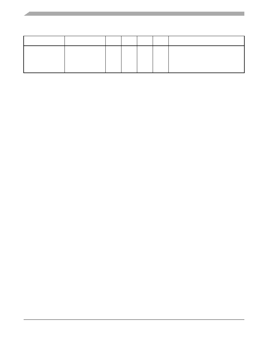
Tcrosslink
Crosslink random
timeout
0
—
1
ms
This random timeout helps resolve
conflicts in crosslink configuration by
eventually resulting in only one
downstream and one upstream port. See
Note 7.
Notes:
1. No test load is necessarily associated with this value.
2. Specified at the measurement point into a timing and voltage compliance test load as shown in Figure 58 and measured over
any 250 consecutive TX UIs. (Also refer to the transmitter compliance eye diagram shown in Figure 56.)
3. A TTX-EYE = 0.70 UI provides for a total sum of deterministic and random jitter budget of TTX-JITTER-MAX = 0.30 UI for the
transmitter collected over any 250 consecutive TX UIs. The TTX-EYE-MEDIAN-to-MAX-JITTER median is less than half of the total
TX jitter budget collected over any 250 consecutive TX UIs. It should be noted that the median is not the same as the mean.
The jitter median describes the point in time where the number of jitter points on either side is approximately equal as
opposed to the averaged time value.
4. The transmitter input impedance shall result in a differential return loss greater than or equal to 12 dB and a common mode
return loss greater than or equal to 6 dB over a frequency range of 50 MHz to 1.25 GHz. This input impedance requirement
applies to all valid input levels. The reference impedance for return loss measurements is 50
Ωto ground for both the D+ and
D– line (that is, as measured by a vector network analyzer with 50-
Ωprobes—see Figure 58.) Note that the series capacitors
CTX is optional for the return loss measurement.
5. Measured between 20%–80% at transmitter package pins into a test load as shown in Figure 58 for both VTX-D+ and VTX-D–.
6. See Section 4.3.1.8 of the PCI Express Base Specifications, Rev 1.0a.
7. See Section 4.2.6.3 of the PCI Express Base Specifications, Rev 1.0a.
Table 59. Differential Transmitter (TX) Output Specifications (continued)
Symbol
Parameter
Min
Nom
Max
Unit
Comments
相关PDF资料 |
PDF描述 |
|---|---|
| MPC8544EAVTANGA | IC MPU POWERQUICC III 783-FCBGA |
| MPC8544EAVTALFA | IC MPU POWERQUICC III 783-FCBGA |
| SLW5S-5C7LF | CONN ZIF CIC 5POS DIP 1MM VERT |
| XF2L-0735-1A | CONNECTOR FPC 7POS 0.5MM SMD |
| XF2L-0725-1A | CONN FPC 7POS 0.5MM PITCH SMD |
相关代理商/技术参数 |
参数描述 |
|---|---|
| MPC8544EAVTARJ | 功能描述:微处理器 - MPU PQ3 8544E Netwrk Comm Indstrl Cntrl RoHS:否 制造商:Atmel 处理器系列:SAMA5D31 核心:ARM Cortex A5 数据总线宽度:32 bit 最大时钟频率:536 MHz 程序存储器大小:32 KB 数据 RAM 大小:128 KB 接口类型:CAN, Ethernet, LIN, SPI,TWI, UART, USB 工作电源电压:1.8 V to 3.3 V 最大工作温度:+ 85 C 安装风格:SMD/SMT 封装 / 箱体:FBGA-324 |
| MPC8544EAVTARJA | 功能描述:数字信号处理器和控制器 - DSP, DSC PQ38K 8544E RoHS:否 制造商:Microchip Technology 核心:dsPIC 数据总线宽度:16 bit 程序存储器大小:16 KB 数据 RAM 大小:2 KB 最大时钟频率:40 MHz 可编程输入/输出端数量:35 定时器数量:3 设备每秒兆指令数:50 MIPs 工作电源电压:3.3 V 最大工作温度:+ 85 C 封装 / 箱体:TQFP-44 安装风格:SMD/SMT |
| MPC8544ECVTALF | 功能描述:微处理器 - MPU PQ38K 8544E RoHS:否 制造商:Atmel 处理器系列:SAMA5D31 核心:ARM Cortex A5 数据总线宽度:32 bit 最大时钟频率:536 MHz 程序存储器大小:32 KB 数据 RAM 大小:128 KB 接口类型:CAN, Ethernet, LIN, SPI,TWI, UART, USB 工作电源电压:1.8 V to 3.3 V 最大工作温度:+ 85 C 安装风格:SMD/SMT 封装 / 箱体:FBGA-324 |
| MPC8544ECVTALFA | 功能描述:数字信号处理器和控制器 - DSP, DSC PQ38K 8544E COMMERCIAL RoHS:否 制造商:Microchip Technology 核心:dsPIC 数据总线宽度:16 bit 程序存储器大小:16 KB 数据 RAM 大小:2 KB 最大时钟频率:40 MHz 可编程输入/输出端数量:35 定时器数量:3 设备每秒兆指令数:50 MIPs 工作电源电压:3.3 V 最大工作温度:+ 85 C 封装 / 箱体:TQFP-44 安装风格:SMD/SMT |
| MPC8544ECVTANG | 功能描述:微处理器 - MPU PQ38K 8544E RoHS:否 制造商:Atmel 处理器系列:SAMA5D31 核心:ARM Cortex A5 数据总线宽度:32 bit 最大时钟频率:536 MHz 程序存储器大小:32 KB 数据 RAM 大小:128 KB 接口类型:CAN, Ethernet, LIN, SPI,TWI, UART, USB 工作电源电压:1.8 V to 3.3 V 最大工作温度:+ 85 C 安装风格:SMD/SMT 封装 / 箱体:FBGA-324 |
发布紧急采购,3分钟左右您将得到回复。