- 您现在的位置:买卖IC网 > PDF目录224505 > MT41J512M4JE-187EIT:A 64M X 4 DDR DRAM, PBGA82 PDF资料下载
参数资料
| 型号: | MT41J512M4JE-187EIT:A |
| 元件分类: | DRAM |
| 英文描述: | 64M X 4 DDR DRAM, PBGA82 |
| 封装: | 12.50 X 15 MM, LEAD FREE, FBGA-82 |
| 文件页数: | 7/11页 |
| 文件大小: | 288K |
PDF: 09005aef826aaadc/Source: 09005aef826a65af
Micron Technology, Inc., reserves the right to change products or specifications without notice.
2Gb DDR3 SDRAM.fm - Rev. C 12/07 EN
5
2006 Micron Technology, Inc. All rights reserved.
2Gb: x4, x8 DDR3 SDRAM
Ball Assignments and Descriptions
Advance
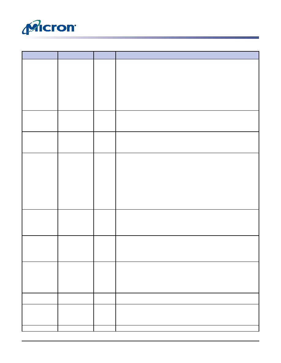
Table 3:
82-Ball FBGA (x4, x8)
Ball Number
Symbol
Type
Description
K4, L8,L4, K3,
L9, L3, M9, M3,
N9, M4, H8, M8,
K8,
N4, N8
A0–A3
A4–A7
A8–A10/AP, A11,
A12/BC#
A13, A14
Input
Address inputs: Provide the row address for ACTIVATE commands, and
the column address and auto precharge bit (A10) for READ/WRITE
commands, to select one location out of the memory array in the
respective bank. A10 sampled during a PRECHARGE command
determines whether the PRECHARGE applies to one bank (A10 LOW,
bank selected by BA0–BA2) or all banks (A10 HIGH). The address inputs
also provide the op-code during a LOAD MODE command. Referenced to
VREFCA. A12/BC#: When enabled in the mode register, A12 is sampled
during READ and WRITE commands to determine whether BC (OTF) will
be performed (HIGH = BL8 or no BC, LOW = BC4).
J3,K9, J4
BA0–BA2
Input
Bank address inputs: BA0–BA2 define the bank to which an ACTIVATE,
READ, WRITE, or PRECHARGE command is being applied. BA0–BA2
define which mode register (MR0, MR1, MR2, or MR3) is loaded during
the LOAD MODE command. Referenced to VREFCA.
F8, G8
CK, CK#
Input
Clock: CK and CK# are differential clock inputs. All control and address
input signals are sampled on the crossing of the positive edge of CK and
the negative edge of CK#. Output data strobe (DQS/DQS#) is referenced
to the crossings of CK and CK#.
G10
CKE
Input
Clock enable: CKE (registered HIGH) activates and CKE (registered LOW)
deactivates internal circuitry and clocks on the DDR3 SDRAM. The specific
circuitry that is enabled/disabled is dependent on the DDR3 SDRAM
configuration and operating mode. Taking CKE LOW provides
PRECHARGE power-down and SELF REFRESH operations (all banks idle),
or active power-down (row active in any bank). CKE is synchronous for
power-down entry and exit and for self refresh entry. CKE is
asynchronous for self refresh exit. Input buffers (excluding CK, CK#, CKE,
RST
#, and ODT) are disabled during power-down. Input buffers
(excluding CKE and RST
#) are disabled during SELF REFRESH. Referenced
to VREFCA.
H3
CS#
Input
Chip select: CS# (registered LOW) enables and (registered HIGH)
disables the command decoder. All commands are masked when CS# is
registered HIGH. CS# provides for external rank selection on systems with
multiple ranks. CS# is considered part of the command code. Referenced
to VREFCA.
B8
DM
Input
Input data mask: DM is an input mask signal for write data. Input data
is masked when DM is sampled HIGH along with that input data during a
write access. Although the DM ball is input-only, the DM loading is
designed to match that of DQ and DQS balls. Referenced to VREFDQ. DM
can also be used as TDQS on the x8.
G2
ODT
Input
On-die termination: ODT (registered HIGH) enables and (registered
LOW) disables termination resistance internal to the DDR3 SDRAM.
When enabled in normal operation, ODT is only applied to each of the
following balls: DQ0–DQ7, DQS, DQS#, and DM for the x8; DQ0–DQ3,
DQS, DQS#, and DM for the x4. The ODT input will be ignored if disabled
via the LOAD MODE command. Referenced to VREFCA.
J4, G4, H4
RAS#, CAS#, WE#
Input
Command inputs: RAS#, CAS#, and WE# (along with CS#) define the
command being entered. Referenced to VREFCA.
N3
RST#
Input
Reset: An active LOW CMOS input is referenced to VSS. The reset input
receiver is a CMOS input defined as a rail-to-rail signal with DC HIGH
≥
0.8 × VDDQ and DC LOW
≤ 0.2 × VDDQ. RST# assertion and desertion are
asynchronous.
B4, C8, C3, C9
DQ0–DQ3
I/O
Data input/output: Bidirectional data bus for x4. Referenced to VREFDQ.
相关PDF资料 |
PDF描述 |
|---|---|
| MT42C8255RG-7TR | 256K X 8 VIDEO DRAM, 70 ns, PDSO40 |
| MT46V32M16TG-75ELIT | 32M X 16 DDR DRAM, 0.75 ns, PDSO66 |
| MT46V32M16BN-5BLIT | 32M X 16 DDR DRAM, 0.7 ns, PBGA60 |
| MT46V32M81AZ4-6T:G | 32M X 4 DDR DRAM, 0.75 ns, PDSO66 |
| MT47H128M8HV-187ELIT:E | 128M X 8 DDR DRAM, 0.35 ns, PBGA60 |
相关代理商/技术参数 |
参数描述 |
|---|---|
| MT41J512M4V79D3WC1 | 制造商:Micron Technology Inc 功能描述:512MX4 DDR3 SDRAM DIE-COM COMMERCIAL 1.5V - Trays |
| MT41J512M4V89C3WC1 | 制造商:Micron Technology Inc 功能描述:512MX4 DDR3 SDRAM DIE-COM COMMERCIAL 1.5V - Bulk |
发布紧急采购,3分钟左右您将得到回复。