- 您现在的位置:买卖IC网 > PDF目录224505 > MT46V32M16BN-5BLIT 32M X 16 DDR DRAM, 0.7 ns, PBGA60 PDF资料下载
参数资料
| 型号: | MT46V32M16BN-5BLIT |
| 元件分类: | DRAM |
| 英文描述: | 32M X 16 DDR DRAM, 0.7 ns, PBGA60 |
| 封装: | 10 X 12.50 MM, LEAD FREE, PLASTIC, FBGA-60 |
| 文件页数: | 1/82页 |
| 文件大小: | 2855K |
| 代理商: | MT46V32M16BN-5BLIT |
当前第1页第2页第3页第4页第5页第6页第7页第8页第9页第10页第11页第12页第13页第14页第15页第16页第17页第18页第19页第20页第21页第22页第23页第24页第25页第26页第27页第28页第29页第30页第31页第32页第33页第34页第35页第36页第37页第38页第39页第40页第41页第42页第43页第44页第45页第46页第47页第48页第49页第50页第51页第52页第53页第54页第55页第56页第57页第58页第59页第60页第61页第62页第63页第64页第65页第66页第67页第68页第69页第70页第71页第72页第73页第74页第75页第76页第77页第78页第79页第80页第81页第82页
09005aef80a1d9e7
512MBDDRx4x8x16_1.fm - Rev. H 7/04 EN
1
2000 Micron Technology, Inc. All rights reserved.
512Mb: x4, x8, x16
DDR SDRAM
DOUBLE DATA RATE
(DDR) SDRAM
MT46V128M4 – 32 MEG x 4 x 4 BANKS
MT46V64M8 – 16 MEG x 8 x 4 BANKS
MT46V32M16 – 8 MEG x 16 x 4 BANKS
Micron Web site: www.micron.com/datasheets
Features
VDD = +2.5V ±0.2V, VDDQ = +2.5V ±0.2V
VDD = +2.6V ±0.1V, VDDQ = +2.6V ±0.1V (DDR400)
Bidirectional data strobe (DQS) transmitted/
received with data, i.e., source-synchronous data
capture (x16 has two – one per byte)
Internal, pipelined double-data-rate (DDR)
architecture; two data accesses per clock cycle
Differential clock inputs (CK and CK#)
Commands entered on each positive CK edge
DQS edge-aligned with data for READs; center-
aligned with data for WRITEs
DLL to align DQ and DQS transitions with CK
Four internal banks for concurrent operation
Data mask (DM) for masking write data (x16 has two
– one per byte)
Programmable burst lengths: 2, 4, or 8
Auto Refresh and Self Refresh Modes
Longer lead TSOP for improved reliability (OCPL)
2.5V I/O (SSTL_2 compatible)
Concurrent auto precharge option is supported
tRAS lockout supported (tRAP = tRCD)
NOTE:
1. Contact Micron for availability of lead-free products
2. Supports PC3200 modules with 3-3-3 timing
3. Supports PC2700 modules with 2.5-3-3 timing
4. Supports PC2100 modules with 2-2-2 timing
5. Supports PC2100 modules with 2-3-3 timing
6. Supports PC2100 modules with 2.5-3-3 timing
7. Supports PC1600 modules with 2-2-2 timing
8. CL = CAS (Read) Latency
9. Minimum clock rate with a 50% Duty Cycle @ CL = 2 (-75E, -
75Z) and CL = 2.5 (-6T,-75), and CL = 3 (-5B)
Options
Marking
Configuration
128 Meg x 4 (32 Meg x 4 x 4 banks)
128M4
64 Meg x 8 (16 Meg x 8 x 4 banks)
64M8
32 Meg x 16 (8 Meg x 16 x 4 banks)
32M16
Plastic Package
66-pin TSOP
TG
66-pin TSOP Lead-free1
P
60-Ball FBGA (10 x 12.5mm)
FN
60-Ball FBGA (10 x 12.5mm) Lead-free1
BN
Timing – Cycle Time
5ns @ CL = 3 (DDR400B)2
-5B
6ns @ CL = 2.5 (DDR333)3 (FBGA only)
-6
6ns @ CL = 2.5 (DDR333)3 (TSOP only)
-6T
7.5ns @ CL = 2 (DDR266)4
-75E
7.5ns @ CL = 2 (DDR266A)5
-75Z
7.5ns @ CL = 2.5 (DDR266B)6,7
-75
Self Refresh
Standard
None
Low-Power Self Refresh
L
Temperature Rating
Standard
None
Industrial Temperature (-40°C to +85°C)
IT
Key Timing Parameters
SPEED
GRADE
CLOCKRATE8
DATA-OUT
WINDOW9
ACCESS
WINDOW
DQS–DQ
SKEW
CL = 2
CL = 2.5
CL = 3
-5B
133 MHz 167 MHz 200 MHz
1.6ns
±0.70ns
+0.40ns
-6
133 MHz 167 MHz
NA
2.1ns
±0.70ns
+0.40ns
6T
133 MHz 167 MHz
NA
2.0ns
±0.70ns
+0.45ns
-75E/
75Z
133 MHz 133 MHz
NA
2.5ns
±0.75ns
+0.50ns
-75
100 MHz 133 MHz
NA
2.5ns
±0.75ns
+0.50ns
128 MEG x 4
64 MEG x 8
32 MEG x 16
Configuration
32 Meg x 4 x 4
banks
16 Meg x 8 x 4
banks
8 Meg x 16 x 4
banks
Refresh Count
8K
Row Addressing
8K (A0–A12)
Bank Addressing
4(BA0, BA1)
Column
Addressing
4K
(A0-A9, A11, A12)
2K
(A0–A9, A11)
1K
(A0–A9)
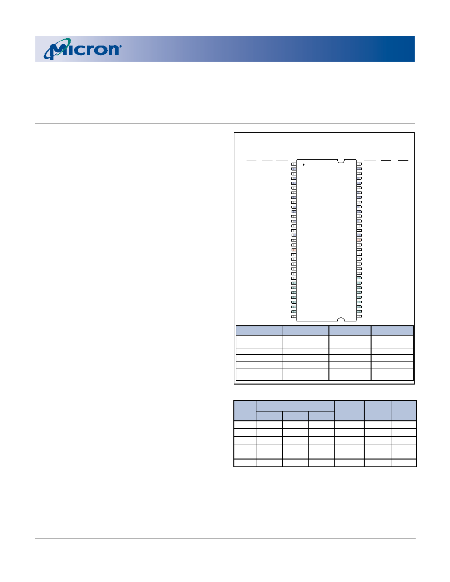
Figure 1: Pin Assignment (Top View)
66-pin TSOP
1
2
3
4
5
6
7
8
9
10
11
12
13
14
15
16
17
18
19
20
21
22
23
24
25
26
27
28
29
30
31
32
33
66
65
64
63
62
61
60
59
58
57
56
55
54
53
52
51
50
49
48
47
46
45
44
43
42
41
40
39
38
37
36
35
34
VSS
DQ15
VSSQ
DQ14
DQ13
VDDQ
DQ12
DQ11
VSSQ
DQ10
DQ9
VDDQ
DQ8
NC
VSSQ
UDQS
DNU
VREF
VSS
UDM
CK#
CK
CKE
NC
A12
A11
A9
A8
A7
A6
A5
A4
VSS
x16
VDD
DQ0
VDDQ
DQ1
DQ2
VssQ
DQ3
DQ4
VDDQ
DQ5
DQ6
VssQ
DQ7
NC
VDD
Q
LDQS
NC
VDD
DNU
LDM
WE#
CAS#
RAS#
CS#
NC
BA0
BA1
A10/AP
A0
A1
A2
A3
VDD
x16
VSS
DQ7
VSSQ
NC
DQ6
VDDQ
NC
DQ5
VSSQ
NC
DQ4
VDDQ
NC
VSSQ
DQS
DNU
VREF
VSS
DM
CK#
CK
CKE
NC
A12
A11
A9
A8
A7
A6
A5
A4
VSS
x8
x4
VSS
NF
VSSQ
NC
DQ3
VDDQ
NC
NF
VSSQ
NC
DQ2
VDDQ
NC
VSSQ
DQS
DNU
VREF
VSS
DM
CK#
CK
CKE
NC
A12
A11
A9
A8
A7
A6
A5
A4
VSS
VDD
DQ0
VDDQ
NC
DQ1
VSSQ
NC
DQ2
VDDQ
NC
DQ3
VSSQ
NC
VDDQ
NC
VDD
DNU
NC
WE#
CAS#
RAS#
CS#
NC
BA0
BA1
A10/AP
A0
A1
A2
A3
VDD
x8
x4
VDD
NF
VDDQ
NC
DQ0
VSSQ
NC
NF
VDDQ
NC
DQ1
VSSQ
NC
VDDQ
NC
VDD
DNU
NC
WE#
CAS#
RAS#
CS#
NC
BA0
BA1
A10/AP
A0
A1
A2
A3
VDD
相关PDF资料 |
PDF描述 |
|---|---|
| MT46V32M81AZ4-6T:G | 32M X 4 DDR DRAM, 0.75 ns, PDSO66 |
| MT47H128M8HV-187ELIT:E | 128M X 8 DDR DRAM, 0.35 ns, PBGA60 |
| MT47H128M8HQ-187ELAT:E | 128M X 8 DDR DRAM, 0.35 ns, PBGA60 |
| MT48LC2M32B1TG-7 | 2M X 32 SYNCHRONOUS DRAM, 5.5 ns, PDSO86 |
| MT48LC32M4A2P-7ELIT:G | 32M X 4 SYNCHRONOUS DRAM, 5.4 ns, PDSO54 |
相关代理商/技术参数 |
参数描述 |
|---|
发布紧急采购,3分钟左右您将得到回复。