- 您现在的位置:买卖IC网 > PDF目录224505 > MT46V32M16BN-5BLIT 32M X 16 DDR DRAM, 0.7 ns, PBGA60 PDF资料下载
参数资料
| 型号: | MT46V32M16BN-5BLIT |
| 元件分类: | DRAM |
| 英文描述: | 32M X 16 DDR DRAM, 0.7 ns, PBGA60 |
| 封装: | 10 X 12.50 MM, LEAD FREE, PLASTIC, FBGA-60 |
| 文件页数: | 11/82页 |
| 文件大小: | 2855K |
| 代理商: | MT46V32M16BN-5BLIT |
第1页第2页第3页第4页第5页第6页第7页第8页第9页第10页当前第11页第12页第13页第14页第15页第16页第17页第18页第19页第20页第21页第22页第23页第24页第25页第26页第27页第28页第29页第30页第31页第32页第33页第34页第35页第36页第37页第38页第39页第40页第41页第42页第43页第44页第45页第46页第47页第48页第49页第50页第51页第52页第53页第54页第55页第56页第57页第58页第59页第60页第61页第62页第63页第64页第65页第66页第67页第68页第69页第70页第71页第72页第73页第74页第75页第76页第77页第78页第79页第80页第81页第82页
512Mb: x4, x8, x16
DDR SDRAM
09005aef80a1d9e7
Micron Technology, Inc., reserves the right to change products or specifications without notice.
512MBDDRx4x8x16_2.fm - Rev. H 7/04 EN
19
2000 Micron Technology, Inc. All rights reserved.
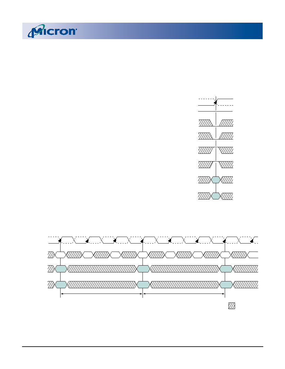
Operations
Bank/Row Activation
Before any READ or WRITE commands can be
issued to a bank within the DDR SDRAM, a row in that
bank must be “opened.” This is accomplished via the
ACTIVE command, which selects both the bank and
the row to be activated, as shown in Figure 10.
After a row is opened with an ACTIVE command, a
READ or WRITE command may be issued to that row,
subject to the tRCD specification. tRCD (MIN) should
be divided by the clock period and rounded up to the
next whole number to determine the earliest clock
edge after the ACTIVE command on which a READ or
WRITE command can be entered. For example, a tRCD
specification of 20ns with a 133 MHz clock (7.5ns
period) results in 2.7 clocks rounded to 3. This is
reflected in Figure 11, which covers any case where 2 <
case for tRCD; the same procedure is used to convert
other specification limits from time units to clock
cycles.)
A subsequent ACTIVE command to a different row
in the same bank can only be issued after the previous
active row has been “closed” (precharged). The mini-
mum time interval between successive ACTIVE com-
mands to the same bank is defined by tRC.
A subsequent ACTIVE command to another bank
can be issued while the first bank is being accessed,
which results in a reduction of total row-access over-
head. The minimum time interval between successive
ACTIVE commands to different banks is defined by
tRRD.
Figure 10: Activating a Specific Row in
a Specific Bank
Figure 11: Example: Meeting tRCD (tRRD) MIN When 2 < tRCD (tRRD) MIN/tCK
≤3
CS#
WE#
CAS#
RAS#
CKE
A0-A12
RA
RA = Row Address
BA = Bank Address
HIGH
BA0, BA1
BA
CK
CK#
t
COMMAND
BA0, BA1
ACT
NOP
RRD
tRCD
CK
CK#
Bank x
Bank y
A0-A12
Row
NOP
RD/WR
NOP
Bank y
Col
NOP
T0
T1
T2
T3
T4
T5
T6
T7
DON’T CARE
NOP
相关PDF资料 |
PDF描述 |
|---|---|
| MT46V32M81AZ4-6T:G | 32M X 4 DDR DRAM, 0.75 ns, PDSO66 |
| MT47H128M8HV-187ELIT:E | 128M X 8 DDR DRAM, 0.35 ns, PBGA60 |
| MT47H128M8HQ-187ELAT:E | 128M X 8 DDR DRAM, 0.35 ns, PBGA60 |
| MT48LC2M32B1TG-7 | 2M X 32 SYNCHRONOUS DRAM, 5.5 ns, PDSO86 |
| MT48LC32M4A2P-7ELIT:G | 32M X 4 SYNCHRONOUS DRAM, 5.4 ns, PDSO54 |
相关代理商/技术参数 |
参数描述 |
|---|
发布紧急采购,3分钟左右您将得到回复。