- 您现在的位置:买卖IC网 > PDF目录224505 > MT46V32M16BN-5BLIT 32M X 16 DDR DRAM, 0.7 ns, PBGA60 PDF资料下载
参数资料
| 型号: | MT46V32M16BN-5BLIT |
| 元件分类: | DRAM |
| 英文描述: | 32M X 16 DDR DRAM, 0.7 ns, PBGA60 |
| 封装: | 10 X 12.50 MM, LEAD FREE, PLASTIC, FBGA-60 |
| 文件页数: | 61/82页 |
| 文件大小: | 2855K |
| 代理商: | MT46V32M16BN-5BLIT |
第1页第2页第3页第4页第5页第6页第7页第8页第9页第10页第11页第12页第13页第14页第15页第16页第17页第18页第19页第20页第21页第22页第23页第24页第25页第26页第27页第28页第29页第30页第31页第32页第33页第34页第35页第36页第37页第38页第39页第40页第41页第42页第43页第44页第45页第46页第47页第48页第49页第50页第51页第52页第53页第54页第55页第56页第57页第58页第59页第60页当前第61页第62页第63页第64页第65页第66页第67页第68页第69页第70页第71页第72页第73页第74页第75页第76页第77页第78页第79页第80页第81页第82页
512Mb: x4, x8, x16
DDR SDRAM
09005aef80a1d9e7
Micron Technology, Inc., reserves the right to change products or specifications without notice.
512MBDDRx4x8x16_2.fm - Rev. H 7/04 EN
64
2000 Micron Technology, Inc. All rights reserved.
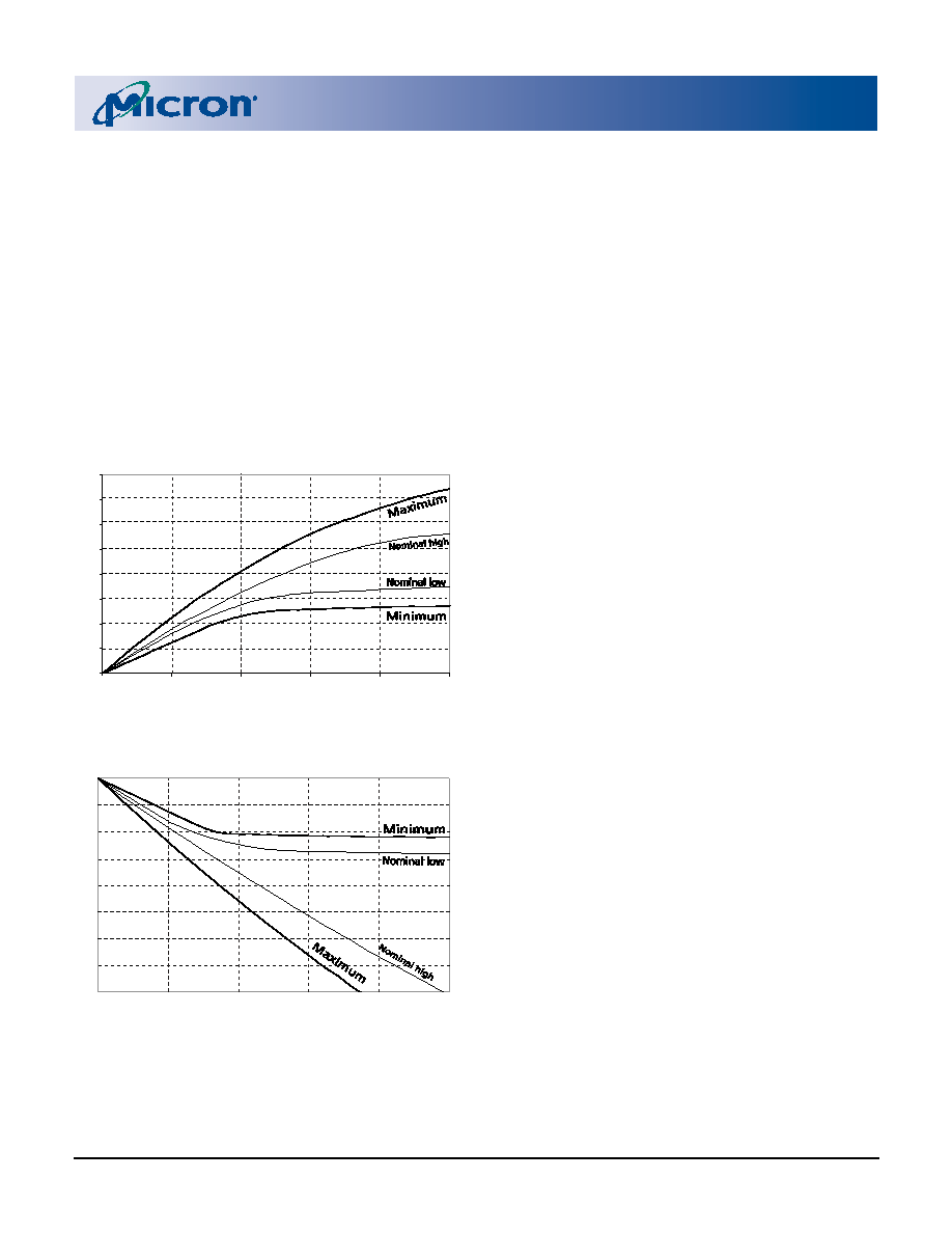
d. The variation in driver pull-up current within
nominal limits of voltage and temperature is
expected, but not guaranteed, to lie within the
inner bounding lines of the V-I curve of
e. The full variation in the ratio of the maximum
to minimum pull-up and pull-down current
should be between 0.71 and 1.4 for device
drain-to-source voltages from 0.1V to 1.0V, and
at the same voltage and temperature.
f. The full variation in the ratio of the nominal
pull-up to pull-down current should be unity
±10 percent, for device drain-to-source volt-
ages from 0.1V to 1.0V.
Figure 38: Reduced Drive Pull-Down
Characteristics
Figure 39: Reduced Drive Pull-Up
Characteristics
39. The voltage levels used are derived from a mini-
mum VDD level and the referenced test load. In
practice, the voltage levels obtained from a prop-
erly terminated bus will provide significantly dif-
ferent voltage values.
40.
VIH overshoot: VIH (MAX) = VDDQ + 1.5V for a
pulse width ≤ 3ns and the pulse width can not be
greater than 1/3 of the cycle rate. VIL undershoot:
VIL (MIN) = -1.5V for a pulse width ≤ 3ns and the
pulse width can not be greater than 1/3 of the
cycle rate.
41. VDD and VDDQ must track each other.
42. tHZ (MAX) will prevail over tDQSCK (MAX) +
tRPST (MAX) condition. tLZ (MIN) will prevail
over tDQSCK (MIN) + tRPRE (MAX) condition.
43. tRPST end point and tRPRE begin point are not
referenced to a specific voltage level but specify
when the device output is no longer driving
(tRPST), or begins driving (tRPRE).
44. During initialization, VDDQ, VTT, and VREF must
be equal to or less than VDD + 0.3V. Alternatively,
VTT may be 1.35V maximum during power up,
even if VDD/VDDQ are 0V, provided a minimum of
42 of series resistance is used between the VTT
supply and the input pin.
45. The current Micron part operates below the slow-
est JEDEC operating frequency of 83 MHz. As
such, future die may not reflect this option.
46. When an input signal is HIGH or LOW, it is
defined as a steady state logic HIGH or LOW.
47. Random addressing changing 50 percent of data
changing at every transfer.
48. Random addressing changing 100 percent of data
changing at every transfer.
49. CKE must be active (HIGH) during the entire time
a refresh command is executed. That is, from the
time the AUTO REFRESH command is registered,
CKE must be active at each rising clock edge, until
tRFC has been satisfied.
50. IDD2N specifies the DQ, DQS, and DM to be
driven to a valid high or low logic level. IDD2Q is
similar to IDD2F except IDD2Q specifies the
address and control inputs to remain stable.
Although IDD2F, IDD2N, and IDD2Q are similar,
IDD2F is “worst case.”
51. Whenever the operating frequency is altered, not
including jitter, the DLL is required to be reset fol-
lowed by 200 clock cycles before any READ com-
mand.
52. This is the DC voltage supplied at the DRAM and
is inclusive of all noise up to 20MHz. Any noise
above 20MHz at the DRAM generated from any
source other than that of the DRAM itself may not
exceed the DC voltage range of 2.6V ±100mV.
53. The -6/-6T speed grades will operate with tRAS
(MIN) = 40ns and tRAS (MAX) = 120,000ns at any
slower frequency.
0
10
20
30
40
50
60
70
80
0.00.5
1.01.5
2.
VOUT (V)
IOU
T
(m
A
)
-80
-70
-60
-50
-40
-30
-20
-10
0
0.0
0.5
1.0
1.5
2.0
2.5
VDDQ - VOUT (V)
IOU
T
(m
A
)
相关PDF资料 |
PDF描述 |
|---|---|
| MT46V32M81AZ4-6T:G | 32M X 4 DDR DRAM, 0.75 ns, PDSO66 |
| MT47H128M8HV-187ELIT:E | 128M X 8 DDR DRAM, 0.35 ns, PBGA60 |
| MT47H128M8HQ-187ELAT:E | 128M X 8 DDR DRAM, 0.35 ns, PBGA60 |
| MT48LC2M32B1TG-7 | 2M X 32 SYNCHRONOUS DRAM, 5.5 ns, PDSO86 |
| MT48LC32M4A2P-7ELIT:G | 32M X 4 SYNCHRONOUS DRAM, 5.4 ns, PDSO54 |
相关代理商/技术参数 |
参数描述 |
|---|
发布紧急采购,3分钟左右您将得到回复。